


2 - 8
2. DEVICE RANGE THAT CAN BE SET
2.1 MELSEC-QnU/DC, Q17nD/M/NC/DR, CRnD-700
2.1 MELSEC-QnU/DC, Q17nD/M/NC/DR, CRnD-700
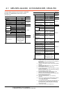
The table below shows the device ranges in [MELSEC-
QnU/DC, Q17nD/M/NC/DR, CRnD-700]
*10
as the
controller type.
*1 Do not set a file register by GT Designer3 when executing
multiple programs with the file of the file register set at [Use
the same file name as the program] by the PLC parameter of
GX Developer.
Otherwise, read/write at GOT will be erroneous.
*2 Available for file register of block No. switched with the RSET
instruction.
*3 Available for file register of block No. of file name switched
with the QDRSET instruction.
*4 GOT treats them in units of 32k (32768 points).
*5 Only the intelligent function module on the station connected
to GOT can be specified.
Set within the address range of the buffer memory existing in
the target intelligent function module.
*6 Do not use local devices set in the MELSEC-Q system.
Otherwise, normal monitoring is not performed.
*7 Even though Universal model QCPU processes 64-bit data,
the GOT cannot monitor 64-bit data.
*8 This is not supported by GT10.
*9 This cannot be monitored when in GOT multi-drop
connection.
*10 For GT14, GT11 and GT10, the controller type is as follows.
• GT14, GT11: MELSEC-QnU/DC, Q17nD/M/NC/DR
• GT10: MELSEC-QnU/DC
*11 For monitoring the internal relay (M) or data register (D) of a
C Controller module, configure the settings related to the
device functions in the device setting tab of the language
controller setting utility.
*12 The device No. must be set in multiples of 16.
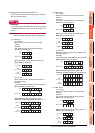
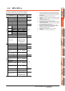
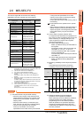
Device name
*7
Setting range
Device No.
representation
Bit device
Input (X) X0 to X3FFF
Hexadecimal
Output (Y) Y0 to Y3FFF
Internal relay (M)
*4*6*11
M0 to M61439
Decimal
Latch relay (L) L0 to L32767
Annunciator (F) F0 to F32767
Link relay (B)
*4
B0 to B9FFFF
Hexadecimal
Timer
*6
Contact (TT) TT0 to TT32767
Decimal
Coil (TC) TC0 to TC32767
Counter
*6
Contact (CT) CT0 to CT32767
Coil (CC) CC0 to CC32767
Special relay (SM) SM0 to SM2255
Retentive
timer
*6
Contact (SS) SS0 to SS32767
Coil (SC) SC0 to SC32767
Step relay (S) S0 to S32767
Link special relay (SB) SB0 to SB7FFF
Hexadecimal
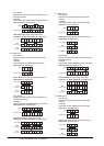
Word device bit
Specified bit of the
following word devices
(Except Timer, Counter,
Retentive timer, Index
register and Buffer
memory)
―
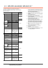
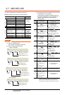
Word device
Data register (D)
*4*6*11
D0 to D4910079
Decimal
Special data register (SD)
SD0 to SD2255
Link register (W)
*4
W0 to W4AEBFF
Hexadecimal
Timer (current value) (TN)
*6
TN0 to TN32767
Decimal
Counter (current value)
(CN)
*6
CN0 to CN32767
Retentive timer
(current value) (SN)
*6
SN0 to SN32767
Link special register (SW)
SW0 to SW7FFF
Hexadecimal
File register (R)
*1*2
R0 to R32767
Decimal
Extension
file register
(ER)
*1
Block 0 to 255
Device ER0 to ER32767
Extension file register
(ZR)
*1*3*4
ZR0 to ZR4849663
Index register (Z) Z0 to Z19
Buffer memory
(Intelligent function module)
(BM)
*5
BM0 to BM32767
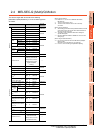
Buffer memory
(Intelligent function module)
(G)
*4*5
G0 to G65535
Ww
*8*9
Ww0 to Ww1FFF
Hexadecimal
Wr
*8*9
Wr0 to Wr1FFF
Multiple CPU high speed
transmission memory (U3E0)
U3E010000 to U3E024335
Multiple CPU high speed
transmission memory (U3E1)
U3E110000
to
U3E124335
Multiple CPU high speed
transmission memory (U3E2)
U3E210000
to
U3E224335
Multiple CPU high speed
transmission memory (U3E3)
U3E310000
to
U3E324335
Motion device (#) #0 to #12287 Decimal
Bit device word
*8*12
Converting the above bit
devices into words
(Except Timer, Counter
and Retentive timer)
―
Device name
*7
Setting range
Device No.
representation