


INTERNAL SPECIFICATIONS
79
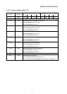
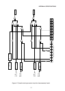
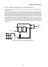
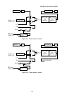
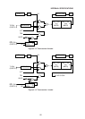
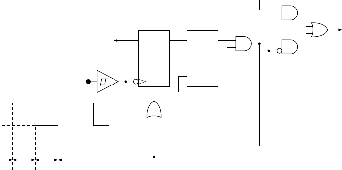
4.5.2.3.1 External clock detector circuit for timer/counters 0 and 1
The detector circuit shown in Figure 4-8 is inserted between the timer/counters and the
external clock pin.
This detector circuit operates in the following way. When the external clock applied to the T0
and T1 pins is changed from “1” to “0” level, that clock is fetched by F/Fl, and is then passed
to F/F2 when the S5 timing signal appears. This F/F2 output is subsequently ANDed (logical
product) with the S3 timing signal to form the timer/counter clock signal which then serves as
the F/Fl reset signal. The reset F/Fl then waits for the next external clock. The “0” and “1” signal
cycle widths of the respective external clocks applied to the T0 and T1 pins must have a
minimum of period 12 times (12T) the XTAL1·2 oscillator clock cycle T. However, when the
CPU is in PD mode or HPD mode the external clock applied to the T0 and T1 pins is input
to timer/counters 0 and 1 directly. The operational time chart for this detector circuit is outlined
in Figure 4-9.
S3
QD
L
QD
R
F/F1 F/F2
S5
T0 or T1
V
CC
RESET
PD & HPD
TIMER 0
or
TIMER 1
1
0
12T 12T
Figure 4- 8 T0 and T1 external clock detector circuit