


MSM80C154S/83C154S/85C154HVS
106
4.6.3 Operating modes
4.6.3.1 Mode 0
4.6.3.1.1 Outline
Mode 0 is the I/O extension mode where input and output of 8-bit data via RXD (P3.0) is
synchronized with the output clock from TXD (P3.1).
The baud rate in mode 0 is fixed to 1/12th of the fundamental oscillator (XTAL1·2) frequency
to enable the serial port to operate synchronized with the basic MSM80C154S/MSM83C154S
timing.
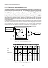
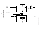
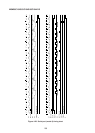
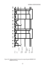
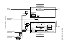
A block diagram of the mode 0 serial port is shown in Figure 4-28, the operational timing chart
is shown in Figure 4-29, and the serial port operation timing in relation to the basic
MSM80C154S/MSM83C154S timing is shown in Figure 4-30.
4.6.3.1.2 Mode 0 baud rate
In mode 0, the baud rate is determined by the following equation to synchronize operations
with the basic MSM80C154S/MSM83C154S timing.
B = FOSC ×
12
1
where B is baud rate, and FOSC is the fundamental (XTAL1·2) frequency.
4.6.3.1.3 Mode 0 transmit operation
Data output is commenced by writing data in SBUF.
The SBUF data is obtained sequentially from RXD about one machine cycle after completion
of the SBUF data writing instruction, the LSB appearing first.
Two states after commencing the LSB output, output of the TXD synchronized clock is
commenced. This synchronized clock is at level “0” from the latter half of S3 thru to the first
half of S6, and at “1” level from the latter half of S6 thru to the first half of S3. The transmit circuit
is initialized immediately following completion of output of the MSB, and the TI flag is set at
the first M1·S3 after that.
4.6.3.1.4 Mode 0 receive operation
Data input is commenced when REN=“1” and R1=“0” is achieved by an instruction used to
set REN or by an instruction used to clear the RI flag (or by an instruction which does both
simultaneously).
Output of the TXD synchronizing clock is commenced following nine states after REN=“1” and
R1=“0” is attained. The synchronized clock is at level “0” from the latter half of S3 thru to the
first half of S6, and at level “1” from the latter half of S6 thru to the first half of S3.
The RXD data is read sequentially into an input shift register in the serial port just before the
synchronized clock is changed from “0” to “1”.
When input of the 8-bit data is completed, loading of the input shift register data into SBUF
(with the LSB at the beginning of the input data) occurs at the same time that receiving circuit
is initialized. The RI flag is then set at the first M1·S3 after completion of input of the 8-bit data.