


MSM80C154S/83C154S/85C154HVS
50
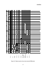
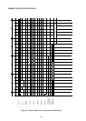
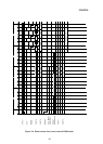
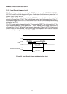
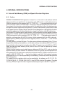
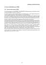
3.2.2 Reset Schmitt trigger circuit
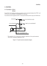
The Schmitt trigger circuit connected to the RESET pin shown in the MSM80C154S/ MSM-
83C154S reset circuit block diagram in Figure 3-4 operates in the following way when the VCC
power supply voltage is +5V.
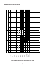
If the voltage of the reset signal applied to the RESET pin exceeds 3V when the level of that
signal is changed from “0” to “1”, the Schmitt trigger output level is changed from “0” to “1”,
and the reset signal is set in the CPU reset control circuit, resulting in the reset operation being
started by the CPU.
The CPU reset state is released when the “1” level on the RESET pin is changed to “0”. An
input signal level below 1.5V is regarded as “0” level, and the Schmitt trigger output level is
changed from “1” to “0”. When the reset signal is changed to “0” level, the CPU reset control
circuit is ready for reset release. The Schmitt trigger circuit operation time chart for changes
in the reset input voltage is outlined in Figure 3-9.
VIH = 3.0[V]
•
•
5 [V]
0 [V]
5 [V]
0 [V]
5 [V]
0 [V]
V
CC
RESET
Schmitt trigger gate output
V
IL = 1.5[V]
•
•
CPU reset
control input
V
TH = 1.5[V]
•
•
Figure 3-9 Reset Schmitt trigger gate detector time chart