


INTERNAL SPECIFICATIONS
55
4. INTERNAL SPECIFICATIONS
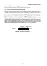
4.1 Internal Data Memory (RAM) and Special Function Registers
4.1.1 Outline
MSM80C154S/MSM83C154S operation is based on an instruction code address method
where operations are specified in an instruction code (OP) section, and the data memory
(RAM) and special function registers (ACC, B, TCON, P0........ ) are specified directly by part
of the instruction code and the second or third byte of data following that instruction code.
According to this instruction code address method, all eight bits of data in the data memory
and special function register may be specified, or one bit of data memory and one bit of data
in the special function register may be specified. Direct designation of all eight bits of data is
called data addressing, and direct designation of one bit of data is called bit addressing.
Since these CPU devices specify data memory (RAM) and special function register contents
by the above method, specific addresses are assigned to the respective CPU data memory
(RAM) and special function registers (ACC, B, TCON, P0, .... ). Data addresses consist of
eight bits, and range from 00 to 0FFH in binary (which correspond to 0 thru 255 in decimal).
All data memory (RAM) and special function registers (ACC, B, TCON, P0, .... ) exist in these
256 locations.
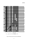
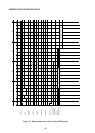
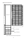
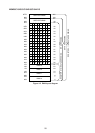
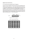
The data memory contains 256 bytes. The data memory between addresses 00 thru 7FH can
be specified directly by data address, and the data memory from address 80H to 0FFH can
be specified by indirect register instruction where R0 or R1 contents are set to 80H thru 0FFH.
Note that the entire data memory (RAM) from 00 thru 0FFH can be specified by indirect
register instruction.
Special function registers are located between addresses 80H thru 0FFH, and can also be
specified directly by data address. Bit addresses consist of eight bits, the manipulation bits
being specified by the three lower order bits and the data memory (RAM) or special function
register (ACC, B, TCON, P0, .... ) by the five higher order bits. Data memory between
addresses 20 thru 2FH can be specified by bit addressing. Other areas cannot be specified
by bit designation.
The special function registers which can be specified by bit address are P0, P1, P2, P3,
TCON, SCON, IE, IP, T2CON, PSW, ACC, B, and IOCON, a total of 13 registers. The data
memory (RAM) and special function register address space layout is shown in Figure 4-1.