


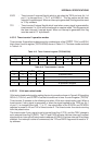
INTERNAL SPECIFICATIONS
97
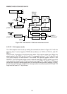
4.5.3.4 Timer/counter 2 detector circuit
4.5.3.4.1 T2 (timer/counter 2 external clock detector)
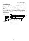
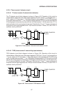
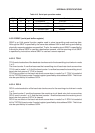
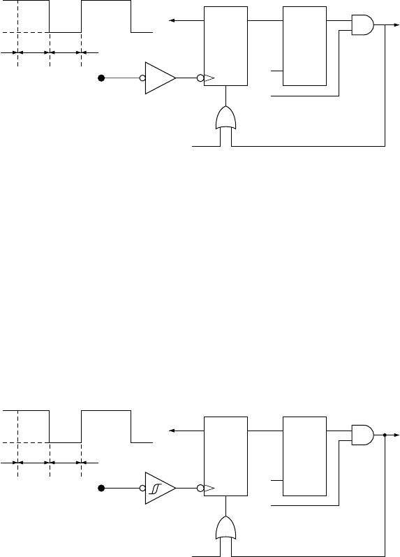
The T2 detector circuit block diagram is shown in Figure 4-23. Operation of this circuit is
outlined below. When the level of the signal applied to T2 (bit 0 of port 1) is changed from “1”
to “0”, output of F/Fl becomes “1”. This output signal is then passed to F/F2 at S5 timing and
F/F2 output also becomes “1”. The T2 signal change passed to F/F2 is synchronized with the
S3 timing signal to become the external clock for timer/counter 2. At the same time, F/F1 is
reset and waits for the next external clock input. Note that the “0” and “1” level cycle times of
the external clock signal applied to the T2 pin must be at least 12 times (12T) the XTAL1·2
oscillator clock cycle time T.
QD
L
QD
R
F/F1 F/F2
S5
T2
[PORT 1.0]
V
CC
RESET
TIMER COUNTER 2
CLOCK
1
0
12T 12T
S3
Figure 4-23 Timer/counter 2 external clock detector circuit
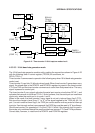
4.5.3.4.2 T2EX (timer/counter 2 external flag input detector)
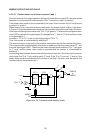
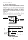
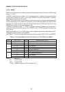
T2EX detector circuit block diagram is shown in Figure 4-24. Operation of this circuit is
outlined below. When the level of the signal applied to T2EX (bit 1 of port 1) is changed from
“1” to “0”, output of F/F1 becomes “1”. This output signal is then passed to F/F2 at S2 timing
and F/F2 output also becomes “1”. The T2EX signal change passed to F/F2 Q is synchronized
with the S4 timing signal to become the T2EX signal for timer/counter 2. At the same time,
F/Fl is reset and waits for the next T2EX input. Note that the “0” and “1” level cycle times of
the external clock signal applied to the T2EX pin must be at least 12 times (12T) the XTAL1·2
oscillator clock cycle time T.
QD
L
QD
R
F/F1 F/F2
S2
T2EX
[PORT 1.0]
V
CC
RESET
TIMER COUNTER 2
T2EX
1
0
12T 12T
S4
Figure 4-24 Timer/counter 2 T2EX detector circuit