Chapter 3: Programming the Peripherals
4538 Hardware Reference Manual 75
T1/E1/J1 Framer Initialization
Introduction
This section details the QuadFALC register initialization, assuming that for non-specified
registers, the initialization is the default value (which is generally 0x00). 4538 Boot
Firmware sources provides routines to initialize the framers in T1/J1 or E1 mode.
Developers should to refer to them.
See Boot Firmware sources: tst\c\qfalc.c)
NOTE
At the end of a QuadFALC port configuration register initialization, it is
recommended that you reset the transmitter and receiver by setting XRES and RRES
bits in CMDR register.
See Boot Firmware sources: tst\c\qfalc.c - Function vFalcWriteCMDR
Master Clock Initialization
The Master Clock provided on the MCLK pin of the QuadFALC devices is at 12.5 MHz.
See Boot Firmware sources: tst\c\qfalc.c - Functions gvQFalcSetPortSyncSrc and
gvQFalcSetPortSyncSrcPT.
TDM Busses General Structure
TDM busses general structure allows four configurations. These different modes are
selected by programming the SWMODE_N (PA7) and COMCLK_N (PA0) signals, the
TDM ports and the QuadFALC registers.
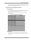
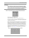
Table 3-1. GCM Register Programming
Register
MCLK
at 12.5 MHz
*&0 [%
*&0 ['
*&0 [$&
*&0 [
*&0 [
*&0 [


