


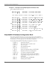


PowerQUICC II CPM Initialization
70 Interphase Corporation
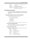
• RFSDx = 01: Receive frame sync delay for TDMa. 01 for 1 clock delay.
• DSCx = 0: Double speed clock for TDMa. 0 means the channel clock rate is
equal to the data clock.
• CTRx = 1: Common receive and transmit pin clocks for TDMa. 1 means Rx and
Tx clocks are common.
• SLx = 1: Sync level for TDMa. 1 means sync active level is 0.
• CEx = 1: Clock edge for TDMa. When DSCx = 1, data sent on the falling edge
and received on the rising edge.
• FEx = 0: Frame Sync edge for TDMa. 0 for falling edge.
• GMx = 0: Grant mode for TDMa. 0 for grant mode not used.
• TFSDx = 01: Transmit frame sync delay for TDMa. 01 for 1 clock delay.
Final Result of SI1AMR register is 0x0171.
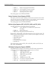
TDM Busses in Independent Direct Mode
According to the TDM busses configuration (VHH7'0%XV&RQILJXUDWLRQV on page 34), the
SI1AMR, SI1BMR, SI2AMR and SI2BMR registers must be set as follows:
• Reserved = 0: This bit should be cleared.
• SADx = 000: Starting bank address for the RAM of TDMAx. 000 for first bank,
first 32 entries.
• SADx = 010: Starting bank address for the RAM of TDMBx. 010 for second bank,
first 32 entries.
• SDMx = 00: SI Diagnostic Mode for TDMx. 00 means normal operation.
• RFSDx = 00: Receive frame sync delay for TDMx. 00 for no clock delay.
• DSCx = 0: Double speed clock for TDMx. 0 means the channel clock rate is
equal to the data clock.
• CTRx = 1: Common receive and transmit pin clocks for TDMx. 1 means Rx and
Tx clocks are common.
• SLx = 1: Sync level for TDMx. 1 means sync active level is 0.
• CEx = 1: Clock edge for TDMx. When DSCx = 0, data sent on rising edge and
received on falling edge.
• FEx = 0: Frame Sync edge for TDMx. 0 for falling edge.
• GMx = 0: Grant mode for TDMx. 0 for grant mode not used.
• TFSDx = 00: Transmit frame sync delay for TDMx. 00 for no clock delay.
Final Result of SI1AMR and SI2AMR registers is 0x0070.
Final Result of SI1BMR and SI2BMR registers is 0x2070.