


Access to the FLASH EEPROM Through PCI
90 Interphase Corporation
When the processor is running, the PCI bus has access to all the elements connected to the
local bus, except the FLASH boot memory: the main SDRAM memory (the processor’s
SDRAM memory controller must be initialized), the QuadFALC framers, etc. (the
processor must have its chip selects programmed). Local space mapping is the same as
when accessed by the processor.
It is not possible to have access to the entire FLASH device when the processor is running,
because the FLASH device is an 8-bit data bus device connected to the 64-bit-only local
bus of the PowerSpan. Only bytes modulo 8 are reachable.
This problem has been neutralized for the other non-64-bit peripherals, by tying their
peripheral address bits 0 to N to the local address bits 3 to N+3 respectively, so that all their
registers can be accessed on byte lane 0, at consecutive modulo 8 addresses.
When the processor is in the reset state, its memory controllers and chip-select signals are
reset, so nothing can be accessed.
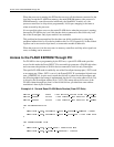
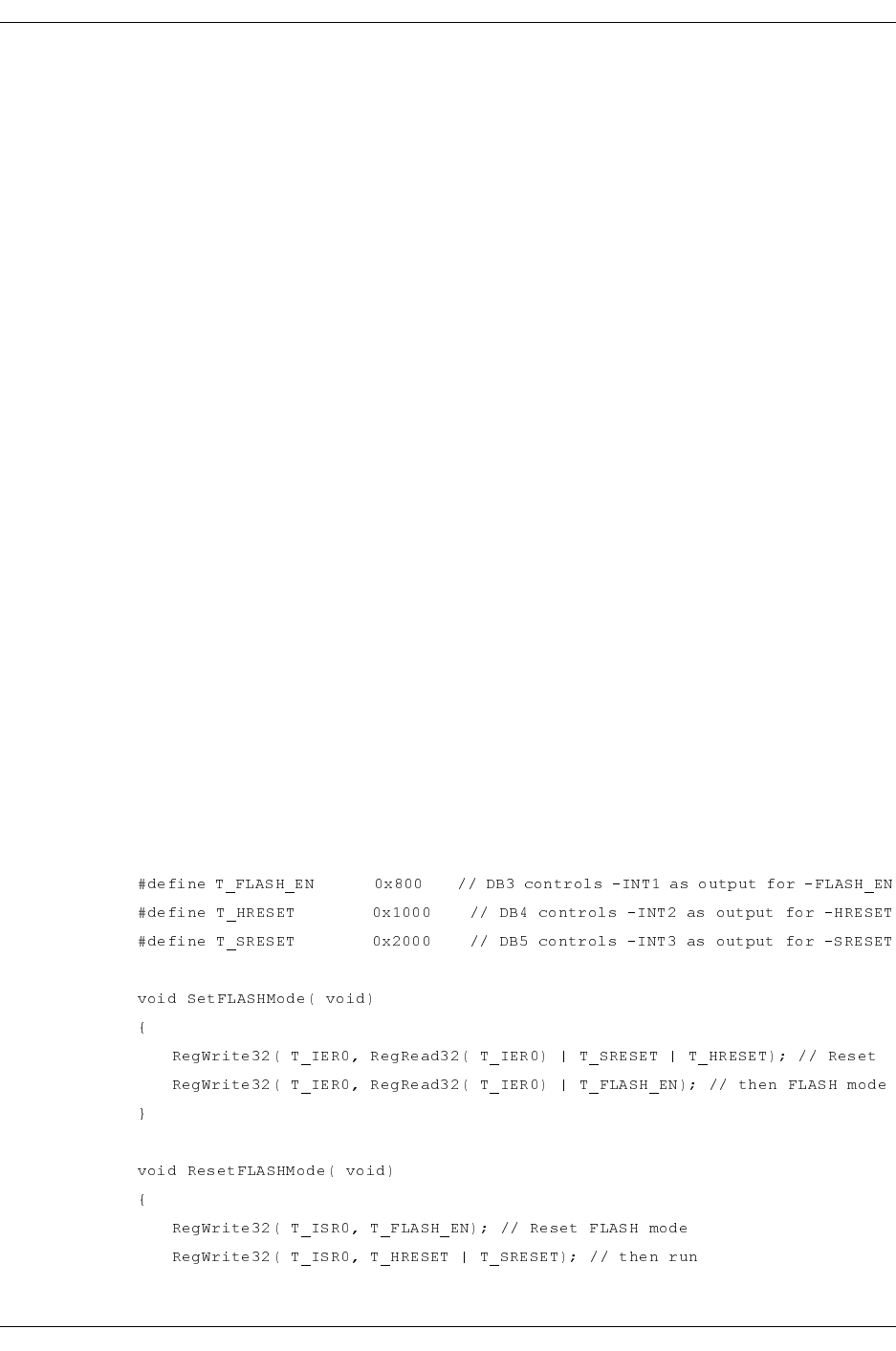
Access to the FLASH EEPROM Through PCI
For FLASH in-situ re-programming by the PCI host, a special FLASH mode provides
access. In this mode, the PowerQUICC II is reset and logic generates a FLASH chip-select
and overcomes the problem of an 8-bit device connected to a 64-bit-only PowerSpan.
The specific FLASH mode is enabled by one of the PowerSpan interrupt pins (–INT1) used
as an output port. When –INT1 is set to 0, the PowerQUICC II is maintained in hard reset
state (–HRESET=0), its pins are tri-stated, the 60x bus is parked for the PowerSpan, and
the following address bus remap is implemented: the device’s low order address bit A (2:0)
is driven by the PowerSpan address bit A (24:22). This remap allows full access of the
FLASH content through byte lane 0 of the 64-bit 60x bus, provided that some address
translation is done by the software.
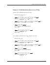
Example 4-4. Set and Reset FLASH Mode Routine (From PCI Side)