


The QuadFALC T1/E1/J1 Framer
30 Interphase Corporation
The FLASH device is normally controlled by the PowerQUICC II memory controller unit
using chip-select signal CS0. The PowerQUICC II can read and re-program the FLASH
using the AMD algorithms.
The FLASH device is not intended to be accessed through the CompactPCI bus. Because
the FLASH device has an 8-bit data bus, and the PowerSpan supports only 64-bit wide
devices, its byte lane can only be accessed by the CompactPCI host for addresses that are
multiples of 8.
For more information, see Access to the FLASH EEPROM Through CompactPCI on page
24.
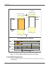
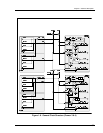
The QuadFALC T1/E1/J1 Framer
The 4538 Communication Controller includes one QuadFALC device which controls four
independent T1/E1/J1 interfaces. For each interface, the QuadFALC includes a framer and
an LIU with data and clock recovery, a frame aligner with two frame elastic buffers for
receive clock wander and jitter compensation, a signaling controller with a HDLC
controller and 64 bytes deep FIFOs, and an 8-bit micro-processor interface.
Each line can be independently configured for E1 or T1. The pulse shape for CEPT E1
applications is programmed according to ITU-T G.703:
• Data Coding: HDB3
• Voltage of nominal pulse: 3 V (CCITT G703)
• Return Loss Transmitter: –12 dB (CCITT G703)
• Line Impedance: 120 Ohm
The pulse shape for T1 applications is programmed according to ANSI T1.403:
• Data Coding: B8ZS
• Voltage of nominal pulse: 3 V
• Return Loss Transmitter: –3.5 dB
• Line Impedance: 100 Ohm
The pulse shape for J1 applications is programmed according to ITU-T JT G.703:
• Data Coding: B8ZS
• Voltage of nominal pulse: 3 V (TBV)
• Return Loss Transmitter: –3.5 dB (TBV)
• Line Impedance: 110 Ohm
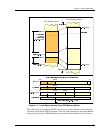
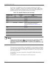
9DOXHVGHSHQGRQ%RRW)LUPZDUHVL]HZKLFKYDU\IURPRQHYHUVLRQWRDQRWKHU±XVHWKH021,725,1)2
FRPPDQGWRGLVSOD\WKHDFWXDOVL]H
Table 1-25. FLASH EEPROM Mapping (cont)
FLASH Addr 1st MAP 2nd MAP Size Description