


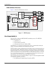

The PowerQUICC II
4 Interphase Corporation
Once all the resets are de-asserted, the PowerQUICC II boots using its 8-bit FLASH device.
The MPC8260 can control the reset of the various communication peripherals through
certain CPM I/O ports. When the PowerQUICC II is in reset state, and until it configures
these I/O ports as outputs, these reset signals are activated.
System Clocks
The MPC8260 gets its reference clock in its CLOCKIN input pin from a 65.536 MHz
reference oscillator.
The MPC8260 input pins MODCK[1:3], along with the MODCK_H field from the Reset
Configuration Word define the input clock used for the SPLL and the default clock
multiplication factors. The resulting internal system frequencies are:
• PowerPC core frequency: 196.608 MHz (x3)
• CPM frequency: 131.072 MHz (x2)
PCI Local Space Mapping
The PowerPC local processor can address a 4 GB logical space. In this space, the following
elements are mapped:
• The vector table (including the reset entry point)
• The MPC8260 internal registers
• The main SDRAM memory
• The FLASH memory
• The PCI bridge (the PowerSpan) and its local-to-PCI window(s)
• The communication peripheral (QuadFALC)
When the MPC8260 boots, it is configured to select the FLASH memory, regardless of the
address generated. This will allow the PowerPC to always find the boot start entry in the
FLASH. After having booted, having executed a proper jump, and initialized the memory
controllers, both the vector table address and the FLASH address can be configured and
mapped in other areas: the developer will typically prefer to implement the vector table in
a R/W memory device (the main memory SDRAM).
The MPC8260 includes 12 banks with their respective Chip Selects.
The memory mapping has been defined in a way that allows use of the MMU Block
Address Translation (BAT) mechanism, which is simpler than the segments-and-pages
mechanism. This mechanism divides the memory into several areas that have their own
cache properties.
Depending on the device selected, the corresponding memory area can be defined as
“cachable” for better performance or must be set as “non cachable”. For instance, the
FLASH memory can be cachable. The areas in the SDRAM that are only accessed by the