Chapter 3: Programming the Peripherals
4538 Hardware Reference Manual 79
RCLK1 is one of the four channels’ internally-generated receive route clocks (RCLK) of a
QuadFALC: the channel selection is set with GPC1.R1S1 and GPC1.R1S0 bits – when
using RCLK1 for synchronizing the TDM SIxRAM, an active channel should be selected.
On each channel, program CMR1.RS1=1 and CMR1.RS0=0: the advantage would be to
have RCLK1 at 2.048 MHz whatever the source’s channel mode is (T1/J1 or E1), the
disadvantage is that in case of an LOS (Loss Of Signal) on the source channel, RCLK1 does
not go to a continuous level, but is the free running frequency of DCO-R. Since DCO-R is
used, program CMR1.DRSS1 and CMR.DRSS0 bits as shown in Table 3-3 to select the
reference source for the DCO-R circuit
SEC/FSC Configuration
The SEC/FSC signal of the QuadFALC is connected to CPM and is used for the TDM frame
synchronization clock (8 KHz synchronization pulse generated by one of the four DCO-
Rs). It must be configured as an FSC output by setting GPC1.CSFP1 to 1. Bit GPC1.CSFP0
allows selecting the active level (low or high). When using the pairing feature, FSC source
must match an active channel as for RCLK1: the source is selected with GPC1.FSS1 and
GPC1.FSS0 bits.
See Boot Firmware sources: TST\C\QFALC.C Function gvQFalcSetPortSyncSrc.
Switched Mode
In switched direct mode, the four framers have the same rhythm. SWMODE_N = 0 and
COMCLK_N = 1.
System Interface
QuadFALC multiplexed bus is connected to the first TDM bus on P4. The second TDM bus
on P4 is connected to the MPC8260. TDM busses clock and frame synchronization signals
are provided by P4.
On QuadFALC, the system multiplex mode must be enabled (GPC1.SMM = 1) with byte
interleaved format (SIC1.BIM=0), clocking rate at 8.192 MHz ( SIC1.SCC1/0=10) and
data rate at 8.192 MBit/s (SIC1.SDD1=1, FMR1.SDD0=0). Time-slot offset programming
was obtained by actual practice: XC0 = 0x00, XC1 = 0x03, RC0 = 0x00, RC1 = 0x03. The
receive buffer size must be set to two frames (SIC1.RBS1/0 = 00). The transmit buffer size
must be set to two frames (SIC1.XBS1/0 = 10). SIC3.RESX and SIC3.RESR must be set
to 0 (Synchronous Pulse Transmit (–SYPX) and Synchronous Pulse Receive
(–SYPR) are latched on first clock (8.192 MHz) rising edge). –SYPX and –SYPR inputs
are mapped to XPA1 and RPA1 pins respectively by setting the PC1 register to 0.
SCLKX_1 and SCLKR_1 must be configured as inputs by setting PC5.CSXP and
PC5.CSRP bits to 0. All these initializations must be performed on each channel.
The multiplexed data stream is internally logically ored. Therefore the selection of the
active channel phase has to be configured differently for each single channel (1–4).
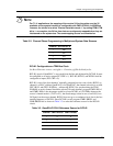
Programming is done with SIC2.SICS2...0 bit as shown in Table 3-2.
See Boot Firmware sources: tst\c\qfalc.c - Functions gvQFalcInitT1, gvQFalcInitJ1 and
gvQFalcInitE1.


