


1999 Apr 14 28
Philips Semiconductors Product specification
Audio processor with head amplifier for VHS hi-fi TDA9605H
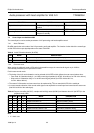
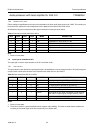
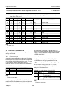
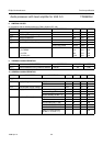
Table 27 Volume left sign (bit VLS), volume left (bits VL5 to VL0), volume right sign (bit VRS) and volume right
(bits VR5 to VR0); note 1
Notes
1. X = don’t care.
2. Power-on reset state.
VLS VL5 VL4 VL3 VL2 VL1 VL0
MODE DESCRIPTION
VRS VR5 VR4 VR3 VR2 VR1 VR0
00000000dB volume 0 dB
0000001−1 dB volume −1dB
0000010−2 dB volume −2dB
:::::::: :
0101110−46 dB volume −46 dB
0101111−47 dB volume −47 dB
011XXXXmute mute
1XX00000dB volume 0 dB; note 2
1XX00011dB volume 1 dB
1XX00102dB volume 2 dB
:::::::: :
1XX111014dB volume 14 dB
1XX111115dB volume 15 dB
7.9 Power byte at subaddress 07H
The power byte is used for power-up settings and the
standby control mode.
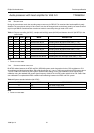
7.9.1 C
ALIBRATION START
Automatic frequency calibration by setting the hi-fi modem,
the band-pass filter and the noise reduction is performed
after a change of bit CALS from logic 0 to logic 1. The use
of auto-calibration is only needed after power-up
(Power-on reset) of the supply voltage (see Section 6.5).
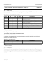
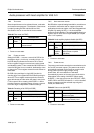
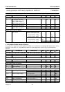
Table 28 Calibration start (bit CALS)
Note
1. Power-on reset state.
The output signal on pin ENVOUT or bit CALR (calibration
ready) and bit CALE (calibration error) of the read byte can
be monitored to check for completion of the calibration.
CALS MODE DESCRIPTION
0 no calibration note 1
1 start
calibration
start of the automatic calibration
cycle
The combination of bit CALR = 1 and bit CALE = 0
indicates a successful calibration. Bit CALS should remain
at logic 1 after the calibration to keep a reliable state of
bit CALR and bit CALE.
7.9.2 DC
OUTPUT VOLTAGE SELECTION
The DC output level on pins LINEL, LINER, DECL
and DECR can be changed by setting bit VCCS to
maximize the output power when using a supply voltage
of 12 V.
The use of power muting (bit MUTE = 1) ensures
disturbance free switching of the line output signal when
setting bit VCCS after power-up.
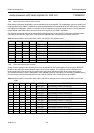
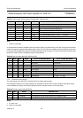
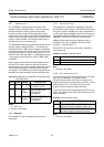
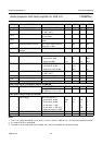
Table 29 V
CC
supply voltage select (bit VCCS)
Note
1. Power-on reset state.
VCCS MODE DESCRIPTION
0 9 V line and decoder output DC voltage
is 4.5 V; note 1
1 12 V line and decoder output DC voltage
is 6 V