


AE/LZB 119 1902 R1A
16
the voltage divider consisting of resistors R202 and R204
and can be metered at test point TP202. The level of this
signal is typically 25 mV RMS. This feedback signal
connects through coupling capacitor C207 to N203, Pin 5
(INM1). The voltage level at this point is typically 4.5 V.
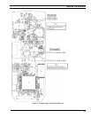
Main Synthesizer (N203)
In synthesizer N203 the feedback signal from the VCO
is input to a prescaler where it is divided down to produce a
19.2 MHz signal. This signal is compared with the 19.2
MHz reference frequency generated by reference oscillator
U201. When these two signals are equal, a lock voltage is
connected through N203, Pin 13 (PHI) or Pin 14 (PHP) to
the selected loop filter, locking the circuit to the output
frequency.
Auxiliary Synthesizer (N203)
The VCO oscillates at the 2nd LO frequency of 75.75
Mhz. A 100 mV
RMS
signal is fed back to N203, Pin
10(INA). This signal is divided down to 12.5 kHz and
phase compared to a 12.5 kHz reference signal which is
derived from the 19.2 Mhz reference oscillator. An error
voltage is generated by any phase error between the two
signals. This error voltage is processed by the loop filter
(R225, R226, C217, C218 and C219) and sent to the voltage
controlled oscillator (VCO). This voltage can be metered at
test point TP209 and is typically 2.5 ± 1.0 volts.
Reference Oscillator (U201)
Reference Oscillator U201 provides a reference
frequency of 19.2 MHz at 1.5 PPM for the Phase-Lock-
Loop circuit in the JACQUI module (the main synthesizer
for the receiver 1st LO, HILLARY and DEBBIE). The
output level of this module is +16 dBM and can be metered
at test point TP204. The output of U201, Pin 3 (Output)
connects through a band-pass filter consisting of capacitor
C235, inductor L202 and capacitor C236. This output then
connects to the JACQUI circuit through the REF_OSC line
and to Frequency Synthesizer N203, Pin 8 (INR) through
coupling capacitor C223. The voltage level on Pin 8 is
typically 330 mV. A buffered output from JACQUI on Pin
19, drives the clock input of HILLARY and DEBBIE. An
Automatic Frequency Control (AFC) line from DEBBIE
(DAC03) provides a control voltage ranging typically from
0.5 volts to 4.5 volts to maintain oscillator integrity. This
DC level adjusts the reference oscillator frequency and is set
by tracking data. Filtering of this line is provided by
capacitors C222 and C234. Supply voltage for U201 is
supplied by synthesizer regulator N290 through the VSYN
line. This voltage connects through resistor R218 to U201,
Pin 4 (Vcc) and is filtered by capacitors C220 and C221.
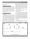
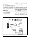
DC POWER DISTRIBUTION
Battery voltage (7.2 Volts) connects to battery
connector X101, the positive terminal (BATT +) Pin 1 and
the negative terminal (BATT -) Pin 3. Fuse F190 and diode
V190 provide short circuit and reverse polarity protection.
If the battery terminals were connected incorrectly (positive
to negative and negative to positive), V190 would conduct
and fuse F190 would blow.
Synthesizer Regulator (N290)
Battery voltage connects through a decoupling circuit
consisting of inductor L290 and capacitor C290 to voltage
regulator N290, Pin 6 (Vin). A PWR ENABLE_B line,
originating from Power Switch V905, connects to N290, Pin
1 (Cntrl). When the Cntrl input is low, N290 is enabled and
a regulated 5.5 Volts is on N290, Pin 4 (Vout). Filtering for
this line is provided by capacitor C291. This voltage can be
metered at test point TP290 and becomes the VSYN line
going to the synthesizer circuit.
Receiver Regulator (N490)
Battery voltage connects through a decoupling circuit
consisting of inductor L490 and capacitor C490 to receiver
voltage regulator N490, Pin 6 (Vin). A RX_ON signal,
generated by D701, connects through enabling switch
transistor V490 to N490, Pin 1 (Cntrl). Resistor R290
connected to the base of transistor V490 is the pull-up
resistor for RX_ON. Regulator N490 is normally enabled.
When RX_ON goes high, V490 conducts and N490 is
enabled. The control voltage can be metered at test point
TP490. With N490 enabled a regulated 5.5 Volts is on
N490, Pin 4 (Vout). This voltage can be metered at TP491.
Capacitor C491 provides line filtering. This voltage
becomes the VREC line going to the receive circuit to
enable the LO buffer, IF Amp 1, IF Amp 2 and IF chip.
Transmit Regulator (N190)
Battery voltage connects through a decoupling circuit
consisting of inductor L190 and capacitor C198 to transmit
voltage regulator N190, Pin 6 (Vin). The PWR_
ENABLE_B line connects to Pin 1 (Cntrl) to enable the
regulator. When the Cntrl is low, the regulator is enabled.
When enabled, a regulated 5.5 Volts is on Pin 4 (Vout).
This voltage can be monitored at test point TP190. Filtering
for this Voltage Transmit (VTX) line is provided by
capacitor C199. The VTX line connects to power control
circuit N102-A, power control buffer N102-B, transistor
switch V153 and TX/Converter/Modulation circuit N150
(JACQUI).