


AE/LZB 119 1902 R1A
15
divider consisting of resistors R116 and R117. The output
of the divider circuit connects to power control buffer
amplifier N102-B, Pin 5 (+IN). The output of N102-B
drives Pin 1 of the power amplifier.
Power Control Buffer (N102-B)
A regulated 5.5 Vdc is applied to power control buffer
N102-B, Pin 8 (V+). The buffer circuit is a shaping circuit
which provides a control voltage on Pin 7 (+OUT). This
voltage after passing through resistor R120 is typically 2.5
Vdc to 3.0 Vdc at 3 watt output and can be metered at test
point TP103. This control voltage connects through filter
capacitor C138, RF choke L113 and resistor R105 to power
amplifier N101, Pin 1 (Pin/Vc). This voltages regulates the
power output of N101. The output of the PA is increased or
decreased by the DC level applied to N102, Pin 1. The
feedback loop is stable when the output power level
produces a detected level equal to the level prestored as a
tracking value equal to 3 watts.
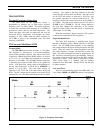
Transmit Low-Pass Filter/Antenna Switch
When the transmit circuit is keyed (Push-To-Talk
switch pressed), SW_B+ (7.0 Vdc) is applied through RF
choke L105 to PIN diode V100. With 7.0 volt applied,
V100 and PIN diode V101 are forward biased. The RF
signal is then allowed to pass through the low-pass filter to
the antenna. The 6.2 volts on the cathode of V100 connects
through inductor L103 to the anode of PIN diode V101.
Capacitor C108, L103 and C109 make a parallel resonant
circuit which prevents RF from flowing into the RX port.
The voltage on the cathode of V101 (5.3 Vdc) connects
through inductor L104, capacitor C112, resistor R100,
capacitor C113 and inductor L107 to the input of the MMIC
buffer amplifier (See MMIC Buffer Amplifier).
Transmit Modulation
The microphone input is through capacitor C300 and
resistor R301 to operational amplifier N300, Pin 2 (-A)
(Refer to Schematic Diagram sheet 10). The output of
N300 is on Pin 1 (Out A). This output is connected to
DEBBIE D601, Pin 19 (AUX). This audio signal is
amplified, limited, passed through a low pass filter and an
encoder circuit where the analog signal is digitized. The
digitized output of the encoder connects through D601, Pin
35 (DPCO) to HILLARY D701, Pin 41 (PCM_CDCMIC)
where it is connected to a PCM interface. The output of the
interface connects through D701, Pin 68 to the DSP module
through X11-18 (See Schematic Diagram, Sheet 13). The
actual connection to the DSP board is at X21-18
(PMC_DSPMIC). The transmit digitized audio can be
metered at test point TP6 on the DSP board. This signal is
then connected to D1, Pin 63 (DR). The audio is filtered
and connected through D1, Pin 133 (TDX) to X21-13
(TXSIF_DSPDATA). This signal can be metered at test
point TP4. This connection then connects through X11-13
to HILLARY D701, Pin 77 where it goes through a TX DSP
INTERFACE. The output of the interface applies the
digitized audio to the input of a sigma/delta modulator or
DAC. In the sigma/delta modulator a sample of the audio is
taken at a 19.2 MHz rate. This generates a pulse that the
width varies with the audio. The outputs of the DAC are
through D701, Pin 15 (MODI), Pin 14 (MODI_B), Pin 16
(MODQ) and Pin 17 (MODQ_B). The pulse rate of each
of these outputs is 9.6 MHz or one-half of the 19.2 MHz
clock rate. These outputs are connected through low pass
filters to the inputs of JACQUI N150 where modulation
takes place. The output of the low pass filters is a true
analog signal consisting of complex wave forms and a pulse
of 800 mV Peak-Peak.
SYNTHESIZER
Dual Synthesizers (N203)
There are two synthesizers in the synthesizer circuit.
One is the main synthesizer which generates the 1st LO
frequency (1011.2 to 1016.2 MHz). The other synthesizer
circuit is the auxiliary synthesizer which generates the 2nd
LO frequency (76.65 MHz). These synthesizer circuits are
programmed by STROBE 1, CLOCK and DATA. These
programming inputs also go to JACQUI. The only
difference is that JACQUI uses STROBE 2. This is so that
when strobed, the programming information gets written to
the proper device. The main synthesizer can be
programmed in 12.5 kHz steps. These inputs can be
metered at TP205 (CLOCK), TP206 (DATA) and TP207
(STROBE 1).
Bilateral Switch (N201)
Bilateral Switch N201 selects the loop filter required
for programming the main VCO in 12.5 kHz steps. A +5
Volt signal (LOOP_SEL) from HILLARY connects to
N201, Pin 5 (2_C
Control
) causing N201 to switch in the
required resistor-capacitor combinations. The selected loop
connects to the VCO at U200, Pin 2 (Vcont).
Main Voltage Controlled Oscillator (U200)
A signal from HILLARY (VCO_BAND_1) turns
transistor V201 on or off to select the band over which the
VCO will operate. The collector output of V201 connects to
U200, Pin 10 (SW). The output of U200 on Pin 8 (Output)
connects through buffer transistor V200 to the RX_ LO
through coupling capacitor C208. The TX_LO is taken
from the voltage divider consisting of resistors R203 and
R205. The feedback for the synthesizer circuit is taken from