


AE/LZB 119 1902 R1A
14
(MODQ and MODQ_B). The I input passes through a low
pass filter consisting of capacitors C191, C192 and C193,
resistor R166 and inductors L156 and L157. The output of
this filter connects to N150, Pins 43 (I) and 42 (I_bar). The
Q input passes through a low pass filter consisting of
capacitors C194, C195 and C196, resistor R167 and
inductor L158 and L159. The output of this low pass filter
connects to N150, Pins 41 (Q) and 40 (Q_bar). The I and
Q inputs are summed with the lower side band then the
outputs of these mixer circuits are summed to produce the
lower side band with transmit modulation. This signal is
amplified and connected through N150, Pin 34 (DUAL TX)
to the input of a transmit band pass filter.
SAW Transmit Band Pass Filter 1
The TX_RF signal (0 dBm) connects through coupling
capacitor C125 to the input of a TX Band Pass Filter.
Filtering of the TX_RF line is provided by capacitor C126.
The lower sideband output of the band pass filter (-8 dB)
connects through coupling capacitors C121 and C139 to the
base of buffer amplifier transistor V104. Filtering is
provided by capacitor C120.
MMIC Buffer Amplifier
When transmitting, the collector voltage for transistor
V104 is provided through PIN diode V101 and is controlled
by DPTT. The RF output from the collector (+3 dBM)
connects through coupling capacitor C116 and resistor R105
to power amplifier N101, Pin 1 (Pin/Vc).
SAW Transmit Band Pass Filter 2
The output of the MMIC Buffer amplifier is fed to the
input of the second SAW BPF. This filter provides further
attenuation for Tx spurions. The output of this filter is fed
to the RF amplifier
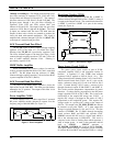
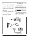
Power Amplifier (N101)
Power amplifier N101 is a three stage Class C operated
RF power amplifier module designed to operate over the
frequency range of 896-940 MHz (see Figure 5).
1
2 34 5
PoutVdd3Vdd2Vdd1Pin/Vc
Figure 5 - Power Amplifier
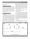
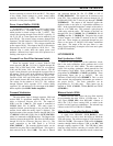
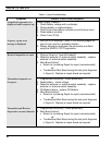
Directional Coupler (W100)
The RF output connected to W100, Pin 4 (PORT 2)
connects directly through W100 to Pin 1 (PORT 1) where it
is output to the antenna circuit. The connection between Pin
9 (PORT 3) and Pin 6 (PORT 4) is part of the sensing
circuit (See Figure 4).
RF Input
RF Output
Port 1 Port 2
Port 3 Port 4
GND GND
50 Ohms
Power Sense
Circuit N102-A
1
Figure 6 - Directional Coupler
Power Sensor Circuit (N102-A)
The power sensor circuit consist of part of W100,
comparator amplifier N102-A and associated circuitry in
between. A regulated 5.5 volts (VTX) from transmit
regulator N190 is applied to N102-A, Pin 8, (V+). This
voltage forward biases Schottky diodes V103-1 and V103-2.
When forward biased diode V103-1 has 0.3 volts on the
anode, a reference voltage of 0.15 volts is on N102-A, Pin 3
(+IN). Forward biasing V103-2 causes a current to flow
through directional coupler W100 (PORT 3 and PORT 4).
This circuit provides temperature compensation for power
detection. A voltage directly proportional to the RF power
output is applied to N102-A, Pin 2 (-IN). This is due to the
rectification of the coupled RF energy into V103-2. A
negative DC voltage is developed at the anode of V103-2
proportional to the coupled RF power. This negative DC
voltage results in a positive DC voltage at the output of
N102-A. This output is the TX_PWR_SENSE line and can
be metered at test point TP102. At 3 watts output this
voltage is typically between 2.8 Vdc and 3.2 Vdc. This line
connects to DEBBIE, Pin 52 (D601) through decoupling
circuit resistors R602 and R603 and capacitor C601.
DEBBIE converts this DC level to a digital word which is
fed to the microprocessor in HILLARY. This word is
compared to the value in Tracking Data which represents 3
watts of output power. A word is then generated and fed
back to DEBBIE. DEBBIE generates a
TX_POWER_CONTROL DC signal on Pin 62 (DAC01).
This signal connects through a decoupling circuit consisting
of resistors R614 and R615 and capacitor C605 to a voltage