MP3 NG: A Next Generation Consumer Platform
XAPP169 (v1.0) November 24, 1999 www.xilinx.com 21
1-800-255-7778
R
When the architecture for this system was being planned, one issue that needed to be
addressed was whether to execute the program image directly from FLASH or to copy it to
SDRAM. There were two key issues that needed to be considered when making this decision.
Performance
The narrow, 8-bit, interface used for both address and data is one performance issue, but it is
not the biggest. The real problem is random access latency. Within a 512-byte memory page,
data can be read with a 50 ns read cycle time. The problem comes when the processor
accesses data on a different page. The time required to load a page into the page register,
where it can be accessed, is 7
µs. With a 66 MHz processor frequency this represents 462
instruction times. This latency will adversely effect real-time performance.
Error Handling
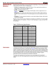
Each 512-byte page in the FLASH has 16 bytes of spare storage for storing ECC information.
The problem is that this is not enough storage for implementing ECC for small block sizes. For
example, to correct single bit errors on an RC32364 cache line (16 bytes) using a Hamming
code the following relationship must be satisfied:
Since there are 32 (512/16) cache lines per page, a total of 36 bytes are needed for ECC
storage. Recall that 16 bytes are available.
In order to get around this problem, the block size could be increased to 32 bytes. At 32 bytes,
ten bits of ECC are required per block, but there are now only 16 blocks per page which is
consistent with the available ECC memory per page. Performing the block check over two
cache lines could accommodate this larger block size. The down side to this is that every time
a cache line is loaded, two would have to be checked with a corresponding increase in memory
latency.
As a result of this the decision was made to copy the executable image to the SDRAM memory
at boot time. This not only increases performance but also turns the ECC checking issue into a
non real-time software exercise.
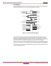
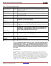
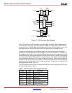
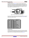
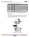
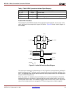
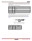
The estimated FPGA device resources used to implement this block include an estimated 100
CLBs, and the ten I/O pads listed in Table 4.
N
≤ 2**K – K – 1
where: N is the number of data bits in the block
K is the number of ECC bits
Solving for K:
16 * 8 = 256
≤ 2K – K – 1
K = 9 ECC bits per cache line
FL_ALE
FL_WE_N
FL_RE_N
FL_SE_N
FL_WP_N
State
Machine
SYS_CLK
FL_R/B_N
FLASH_SEL_N
WR_IN_N[3:0]
ACK_N
RD_IN_N
FL_CE_N[3:0]
Device decodes
from
IP Bus Controller
Figure 20: FLASH Controller Block Diagram


