


18 www.xilinx.com XAPP169 (v1.0) November 24, 1999
1-800-255-7778
MP3 NG: A Next Generation Consumer Platform
R
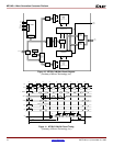
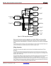
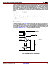
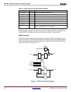
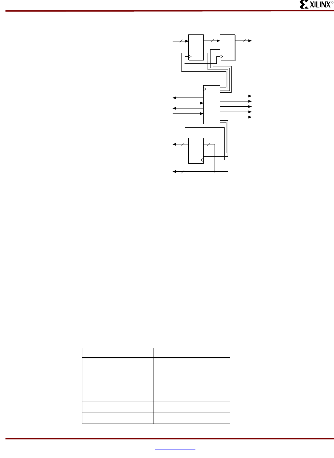
The LCD Controller is an IP bus master and fetches data for screen refresh independently of
CPU activities. The display data that is fetched is loaded into a FIFO using a block transfer
across the IP bus. The shift register loads display data from the FIFO and shifts it out as a 4-bit
wide data stream at 16 MHz the maximum shift rate supported by the display drivers.
In order to prevent disruption of the display image, the FIFO must have a new data word
available for the shift register every time it empties. This occurs every 500 ns (1 / [16 MHz / 8]).
Since there is a significant amount of overhead associated with each non-sequential access to
the SDRAM memory, fetches are made from it using multi-word bursts. The size of these bursts
is a compromise between different factors. Longer bursts are more efficient since the SDRAM
access overhead is amortized over a larger number of data words. Smaller bursts reduce the
size of the FIFO and also reduce bus latency by reducing the time that the LCD controller ties
up the IP bus. For this application a 2-word burst was chosen. The result is a 3-word deep FIFO
and display buffer fetches every 1
µs.
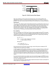
The FPGA device resources used to implement this block include an estimated 58 CLBs and
the nine I/O pads listed in Table 2.
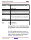
Table 2: LCD Controller Interface Signal Summary
Signal Type Description
DI_XD[3:0] Output X driver data
DI_XSCL Output X driver data shift clock
DI_LP Output Latch pulse
DI_FR Output Frame signal
DI_YD Output Y driver scan start pulse
DI_YSCL Output Y driver shift clock
DIN[31:0]
32
FIFO
Shift
Register
RdWr
32
DQ
Load
Enable
4
DQ
DI_D[3:0]
DI_XSCL
DI_LP
DI_FR
DI_YD
DI_YSCL
State
Machine
9
Load
Enable
9
DQ
SYS_CLK
BREQ_N
BGNT_N
ACK_N
RD_N
Address
Counter
AOUT[10:2]
Base
Address
9
21
AOUT[31:11]
Figure 17: LCD Controller Block Diagram