


MP3 NG: A Next Generation Consumer Platform
XAPP169 (v1.0) November 24, 1999 www.xilinx.com 17
1-800-255-7778
R
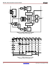
There is no direct software support required for this block, but the USB interface itself requires
considerable software for operation. This software consists of the USB protocol stack, which
includes a USB interrupt service routine. The USB stack itself consists of two parts. The first of
these is the software required for participating in the USB protocol and the plug and play. The
second part is the application specific code required to transfers MP3 files from the host system
to the player.
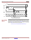
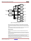
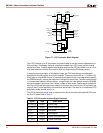
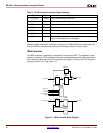
LCD Controller
The LCD Controller is responsible for refreshing the screen with an image stored in the
SDRAM. In general its operation is similar to that of a CRT display controller. Unlike most
display controllers, the display format generated by the LCD controllers is not programmable by
the CPU. The raster format is fixed at 128 x 128 pixels and the display timing is fixed as well.
This makes sense in an embedded system such as this where the display is integrated into the
unit. Although the display format cannot be changed in the system, loading different FPGA
configurations into the FLASH when the unit is manufactured can accommodate different
displays. Figure 17 shows the block diagram of the LCD Controller.
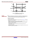
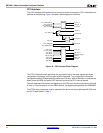
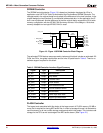
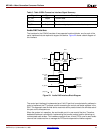
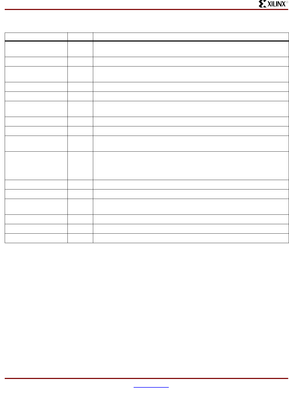
Table 1: CPU Interface Signal Summary
Signal Type Description
CPU_MASTERCLK Output All bus timing is relative to this clock. The CPU core frequency is derived by
multiplying this clock.
CPU_AD[31:0] I/O High-order multiplexed address and data bits.
CPU_ADDR[3:2] Input Non-multiplexed address lines. These serve as the word within block address for
cache refills (Addr[3:2]).
CPU_BE_N[3:0] Input Indicates which byte lanes are expected to participate in the transfer.
CPU_ALE Input Address latch enable.
CPU_CIP_N Input Denotes that a cycle is in progress. Asserted in the address phase and is asserted
until the ACK* for the last data is sampled.
CPU_RD_N Input This active Low signal indicates that the current transaction is a read.
CPU_WR_N Input This active Low signal indicates that the current cycle transaction is a write.
CPU_BUSGNT_N Output During the power-on reset (Cold Reset), BusGnt* is an input and is used to load
ModeBit(5).
CPU_ACK_N Output On read transactions, this signals the RC32364 that the memory system has placed
valid data on the A/D bus, and that the processor may move the data into the on-
chip Read Buffer. On a write transaction, this signals to the RC32364 that the
memory system has accepted the data on the A/D bus.
CPU_RESET_N Output This active Low signal is used for both power-on and warm reset.
CPU_COLDRESET_N Output This active Low signal is used for power-on reset.
CPU_INT_N[3:0] Output Active Low interrupt signals to the CPU. During power-on,
Int*(3:0)serves as
ModeBit(9:6).
US_CS_N Output USB controller chip select.
US_RD_N Output USB controller read strobe.
US_WR_N Output USB controller write strobe.