MP3 NG: A Next Generation Consumer Platform
XAPP169 (v1.0) November 24, 1999 www.xilinx.com 15
1-800-255-7778
R
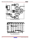
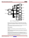
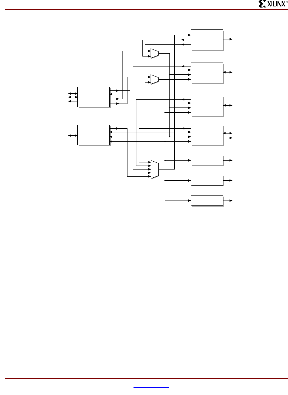
While most of the blocks are fairly independent, the FLASH, SDRAM, and CompactFlash
interfaces share common address and data busses. While this results in a fairly complex
muxing scheme for these datapaths it is necessary to keep the pin count within an acceptable
range.
The following sections will discuss the implementation of each of these functional blocks and
outline the hardware and software resources needed to support each.
IP Bus Controller
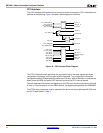
The IP Bus Controller block performs two functions: block address decoding and IP bus
arbitration.
The address decode block generates device selects for the IP block that is the target of the
transfer. It also controls the multiplexers that select the response signals from the target of the
transfer (ACK, DOUT, etc.).
IP bus arbitration between access requests from the CPU Interface and the LCD Controller are
handled by using a simple rotating priority scheme. The arbiter block also controls the
multiplexers that select which set of transfer control signals (RD, WR, etc.) control the transfer.
The FPGA device resources used to implement this block include an estimated 32 CLBs but no
I/O pads. There is no software required to support this block.
CPU Control
D_OUT[31:0]
D_IN[31:0]
A_OUT[31:2]
Control Out
CPU Address/Data
CPU Interface
D_OUT[31:0]
D_IN[31:0]
A_IN[3:2]
Control In
Tranceiver Interface
Signals
IRDA Controller
USB Control
D_IN[31:0]
A_OUT[31:2]
Control Out
LCD Control
Signals
LCD Controller
D_OUT[31:0]
D_IN[31:0]
A_IN[3:2]
Control In
DAC Interface
Signals
DAC Interface
D_OUT[31:0]
D_IN[31:0]
A_IN[3:2]
Control In
ADC Interface
Signals
Touch Screen
Interface
Control In
SDRAM Control
Signals
SDRAM Controller
Control In
FLASH Control
Signals
FLASH Controller
Control In
CompactFlash
Control
Signals
CompactFlash
Controller
MUX
D_OUT[31:0]
D_IN[31:0]
A_IN[19:0]
Control In
Memory Data
Memory Interface
Memory Address
MUX
MUX
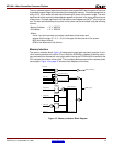
Figure 15: FPGA Logic Block Diagram


