20 www.xilinx.com XAPP169 (v1.0) November 24, 1999
1-800-255-7778
MP3 NG: A Next Generation Consumer Platform
R
SDRAM Controller
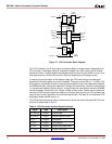
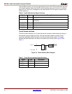
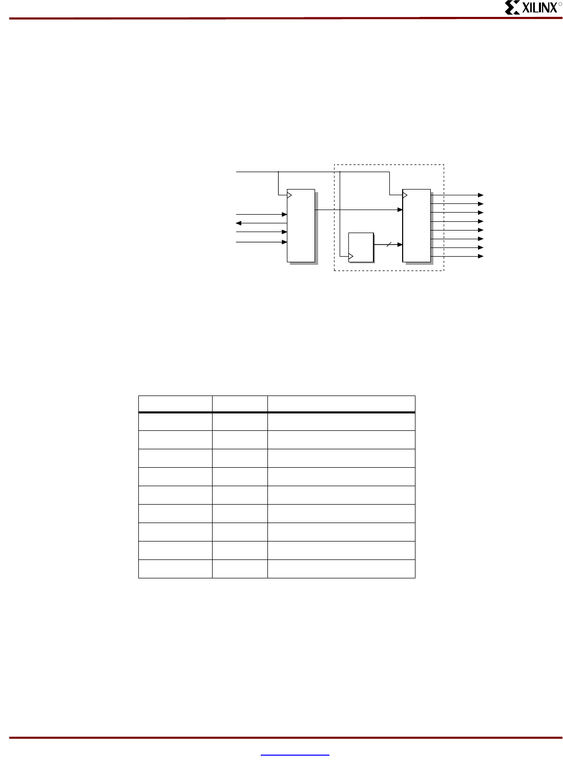
The SDRAM controller design (Figure 19) is based on the design developed by Xilinx in
application note XAPP134: Virtex Synthesizable High Performance SDRAM Controller. The
changes made in the original design are to adapt to the differences in the host interface. In the
original design the host interface is a multiplexed address data bus. In this application the IP
bus is non-multiplexed. Another difference is that the original design supported a 32-bit wide
memory configuration with two MT48LC1M16 memory devices. In the design a 16-bit wide
memory datapath and a single MT48LC1M16 is used.
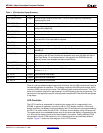
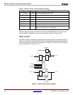
The estimated FPGA device resources used to implement this block include an estimated 100
CLBs, two DLLs, two global clock buffers and the nine I/O pads listed in Table 3 . There is no
software support required for this block.
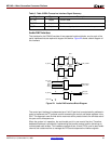
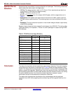
FLASH Controller
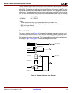
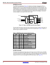
The largest cost associated with this design is the large amount of FLASH memory, 32 MB or
more, that is required for storing MP3 audio files. In order to leverage this cost it is desirable to
use this memory for all non-volatile storage requirements within the system. This includes code
storage for the CPU as well as storage of the MP3 audio stream. (See Figure 20.)
Table 3: SDRAM Controller Interface Signal Summary
Signal Type Description
SD_BA Output Bank address
SD_CS Output Chip select
SD_CLK Output Transfer clock
SD_CKE Output Clock enable
SD_RAS Output Row address strobe
SD_CAS Output Column address strobe
SD_WE Output Write enable
SD_DQML Output Lower byte data mask
SD_DQMH Output Higher byte data mask
32
SD_BA
SA_CS
SD_CLK
SD_CKE
SD_RAS
State
Machine
SYS_CLK
SD_CAS
SD_WE
SD_DQML
SDRAM_SEL_N
WR_IN_N[3:0]
ACK_N
Refresh
Counter
State
Machine
sdrm_t.v from XAPP 134
RD_IN_N
Figure 19: Figure 19 SDRAM Controller Block Diagram


