


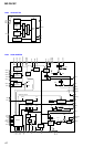
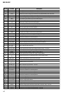
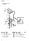

50
MZ-DH10P
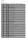
Pin No.
Pin Name I/O Description
306
FS256 O Master clock signal (256Fs=11.2896 MHz) output to A/D converter
307
ADDT I Data input from A/D converter
308
LRCK O L/R sampling clock signal (44.1kHz) output to the A/D converter or D/A converter Not used
309
XBCK O Bit clock (2.8224 MHz) output to the A/D converter or D/A converter Not used
310
OSCI I Main system clock input terminal (22.5792 MHz)
311
OSCO O Main system clock output terminal (22.5792 MHz)
312
FS512 O Clock signal (512Fs=22.5792 MHz) output to the headphone amplifier
313
DTCK I/O TSB master data clock input/output or SSB data input/output with the remote commander
314
UDP I/O USB data (+) input/output terminal
315
UDM I/O USB data (-) input/output terminal
316
USBHOLD I USB hold signal input from the power control IC
317
SUSPEND O USB suspend signal output to the power control IC
318
UPUEN O USB pull-up resistor connection control terminal
319
UOSCI I System clock input terminal (48 MHz) (for USB oscillation circuit)
320
UOSCO O System clock output terminal (48 MHz) (for USB oscillation circuit)
321
EBA0 O Address signal output terminal Not used
322 to 342
EBA1 to EBA21 O Address signal output to the flash memory
343, 344
EBA22, EBA23 O Address signal output terminal Not used
345 to 360
EBD0 to EBD15 I/O Two-way data bus with the flash memory
361 to 376
EBD16 to EBD31
I/O Two-way data bus terminal Not used
377
EBWAIT O Wait signal output terminal Not used
378
EBCS0 O Chip select signal output to the flash memory
379 to 383
EBCS1 to EBCS5
O Chip select signal output terminal Not used
384
EBRD O Read signal output to the flash memory
385
EBWE O Write signal output to the flash memory
386 to 389
EBWR0 to EBWR3
O Access signal output terminal Not used
390 to 392
NC - Not used