


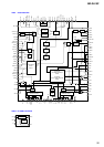
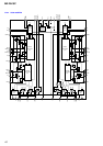
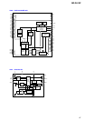
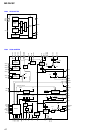
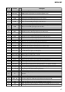
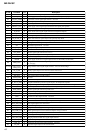
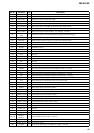
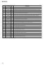

47
MZ-DH10P
Pin No.
Pin Name I/O Description
149
VREFR I Reference voltage input terminal (for internal D/A converter R-CH) Not used
150
DCLSOUTR O PWM modulator signal output to the headphone amplifier (R-CH)
151
DCLSOUTL O PWM modulator signal output to the headphone amplifier (L-CH)
152
RTCK O Not used
153
ADFG I ADIP duplex FM signal (21.05kHz to 23.05 kHz) input from the RF amplifier
154
TRDR O Tracking servo drive PWM signal output (-) to the coil driver
155
TFDR O Tracking servo drive PWM signal output (+) to the coil driver
156
FFDR O Focus servo drive PWM signal output (+) to the coil driver
157
FRDR O Focus servo drive PWM signal output (-) to the coil driver
158
FS4 O 176.4 kHz clock signal output to the over write head driver and power control IC
159
SFDR O Sled servo drive PWM signal output to the motor driver
160
SPDU O Spindle motor drive control signal output (U) to the motor driver
161
SPFD O Spindle servo drive PWM signal output to the motor driver
162
SPDV O Spindle motor drive control signal output (V) to the motor driver
163
SPDW O Spindle motor drive control signal output (W) to the motor driver
164
SPCU I Spindle motor drive comparison signal input (U) from the motor driver
165
SPCV I Spindle motor drive comparison signal input (V) from the motor driver
166
SPCW I Spindle motor drive comparison signal input (W) from the motor driver
167
SLDV O Sled motor drive control signal output (V) to the motor driver
168
SLDW O Sled motor drive control signal output (W) to the motor driver
169
SLCU I Sled motor drive comparison signal input (U) from the motor driver
170
SLCV I Sled motor drive comparison signal input (V) from the motor driver
171
SLCW I Sled motor drive comparison signal input (W) from the motor driver
172
SLDU O Sled motor drive control signal output (U) to the motor driver
173
DIN I Digital audio signal input terminal Not used
174
FS256_OUT O 11.2896 MHz clock output to the RF amplifier
175
CHOPPERCLK O Clock signal output for chopper to the over write head driver
176 to 179
MNT0 to MNT3 O Monitor output terminal for DSP Not used
180
OFTRK I/O Tracking signal input/output for MD3 with the RF amplifier
181
RECP O Laser power selection signal output to the power control IC
182
EFMO O EFM encode data output for the recording to the over write head driver
183
HI_Z_SPDL O Standby signal output for the spindle motor to the motor driver
184
PROTECT I Recording protector for normal disc detection switch input terminal
185
OPT_DET I Optical digital input plug detection signal input terminal "H": optical in Not used
186
XJACK_DET I Line input plug detection signal input terminal "L": plug in Not used
187
XMIC_DET I Microphone input plug detection signal input terminal "L": plug in Not used
188
OPEN_CLOSE_SW
I Top panel open/close detection switch input terminal
189
XCS_ADC O Chip select signal output to the A/D converter Not used
190
XPD_ADC O Power control signal output to the A/D converter Not used
191
NC - Not used
192
XRST_LCD O LCD reset signal output terminal Not used
193
USB_WAKE O System wake up signal output terminal by USB connection
194
A7CAL_SW O A7 offset voltage CAL on/off control signal output to the charge control IC
195
SI0 I Serial data input from the real time clock and EEPROM
196
SO0 O Serial data output to the real time clock, EEPROM and power control IC
197
SCK0 O Serial data transfer clock signal output to the real time clock, EEPROM and power control IC
198
XGUM_ON I Rechargeable battery insert detection switch input terminal