


40
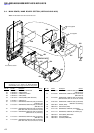
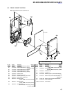
NW-A805/A806/A808/NWZ-A815/A816/A818
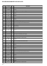
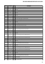
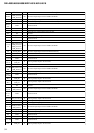
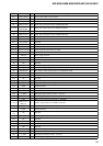
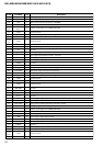
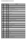
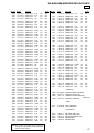
MAIN BOARD IC803 XC2C64A-7CPG56C-01 (LEVEL SHIFT)
Pin No. Pin Name I/O Description
A1 to A4
R3_OUT to
R0_OUT
OVideo signal (R) output to the liquid crystal display
A5 G5_OUT
OVideo signal (G) output to the liquid crystal display
A6 TDO
OData output terminal for JTAG Not used
A7, A8
G2_OUT,
G0_OUT
OVideo signal (G) output to the liquid crystal display
A9, A10
B5_OUT,
B4_OUT
OVideo signal (B) output to the liquid crystal display
B1
R4_OUT O Video signal (R) output to the liquid crystal display
B10 B3_OUT
OVideo signal (B) output to the liquid crystal display
C1
R5_OUT O Video signal (R) output to the liquid crystal display
C3
DATA_IN - Not used
C4, C5
G4_OUT,
G3_OUT
OVideo signal (G) output to the liquid crystal display
C6 VCCIO2
- Power supply terminal
C7 GND -
Ground terminal
C8 G1_OUT
OVideo signal (G) output to the liquid crystal display
C10 B2_OUT
OVideo signal (B) output to the liquid crystal display
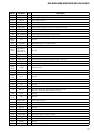
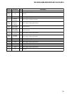
D1
PXCLK_OUT
O
Clock signal output to the liquid crystal display
D3
VAUX
-
Power supply terminal
D8, D10
B1_OUT,
B0_OUT
O
Video signal (B) output to the liquid crystal display
E1
VSYNC_OUT
O
Vertical sync signal output to the liquid crystal display
E3
ERR_IN I Not used
E8
DATA_OUT - Not used
E10
VSYNC_IN
I
Vertical sync signal input from the system controller
F1
HSYNC_OUT
O
Horizontal sync signal output to the liquid crystal display
F3
R4_IN
I
Video signal (R) input from the system controller
F8 GND -
Ground terminal
F10
HSYNC_IN
I
Horizontal sync signal input from the system controller
G1, G3
R5_IN, R2_IN
I
Video signal (R) input from the system controller
G8
VCC - Power supply terminal
G10
B0_IN
I
Video signal (B) input from the system controller
H1, H3
R3_IN, R0_IN
I
Video signal (R) input from the system controller
H4 GND -
Ground terminal
H5
PXCLK_IN
I
Clock signal input from the system controller
H6 VCCIO1
- Power supply terminal
H7, H8,
H10
B4_IN, B2_IN,
B1_IN
I
Video signal (B) input from the system controller
J1
R1_IN
I
Video signal (R) input from the system controller
J10
TDI
I
Data input terminal for JTAG Not used
K1 to K6
G5_IN to G0_IN
I
Video signal (G) input from the system controller
K7, K8
B5_IN, B3_IN
I
Video signal (B) input from the system controller
K9
TMS
I
MS signal input terminal for JTAG Not used
K10
TCK
I
Clock signal input terminal for JTAG Not used