


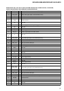
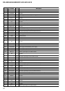
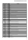
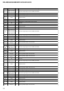

31
NW-A805/A806/A808/NWZ-A815/A816/A818
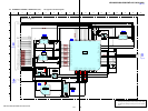
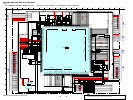
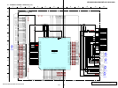
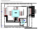
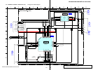
MAIN BOARD IC601 MC-10051F1-FAE-A (SYSTEM CONTROLLER, POWER CONTROL, LCD DRIVER,
NAND FLASH INTERFACE, MS INTERFACE, SD-RAM INTERFACE)
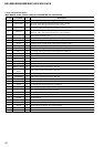
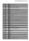
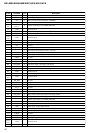
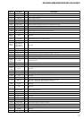
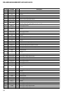
Pin No. Pin Name I/O Description
A1 to A3
NC
-
Not used
A4
NAND_WEZ O Write enable signal output to the NAND flash memory
A5 IO_B -
Not used
A6 to A10
NC
-
Not used
A11 to
A13
GND
-
Ground terminal
A14 to
A16
NC
-
Not used
A17
VCCVBUS
-
Power supply terminal (USB power supply)
A18
NC
-
Not used
A19
IO_A
-
Not used
A20
VDD_L0
-
Power supply terminal
A21 AB0_A8 O
Address signal output to the USB controller
A22 to
A26, B1,
B2
NC -
Not used
B3
NAND_CEZ2 O Chip enable signal output to the NAND flash memory
B4
NAND_DA0 I/O Serial date input/output with the NAND flash memory
B5 IO_B -
Not used
B6
KEY_AD1 I Key input terminal (A/D input)
B7, B8
ADIN6, ADIN8
-
Not used
B9
ADVCC
-
Power supply terminal
B10
CPEN
-
Not used
B11, B12
GND
-
Ground terminal
B13
SWGND
-
Ground terminal
B14
NC
-
Not used
B15
SWADP2
-
Not used
B16
GND
-
Ground terminal
B17
VCCADP
-
Power supply terminal
B18
NC
-
Not used
B19
IO_A
-
Not used
B20
VDD_L0
-
Power supply terminal
B21 to
B26, C1
NC -
Not used
C2, C3
NAND_CEZ1,
NAND_CEZ3
O
Chip enable signal output to the NAND flash memory
C4
NAND_DA1 I/O Serial date input/output with the NAND flash memory
C5 IO_B -
Not used
C6
KEY_AD0 I Key input terminal (A/D input)
C7
ADIN5
-
Not used
C8
CRD_AD I Terminal for peropherals distinction of WM-port
C9
ADGND
-
Ground terminal
C10
NC
-
Not used
C11
GND
-
Ground terminal
C12
NC
-
Not used
C13
GND
-
Ground terminal