


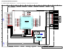
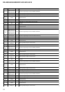
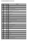

34
NW-A805/A806/A808/NWZ-A815/A816/A818
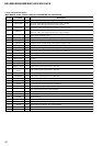
Pin No. Pin Name I/O Description
K4, K5
SDR_DATA28,
SDR_DATA26
I/O Serial data input/output with the 256Mbit SD-RAM
K8
NAND_RBZ3 O Read/busy signal outoput to the NAND flash memory
K9
NAND_DA6
I/O
Serial date input/output with the NAND flash memory
K10 to
K18
GND
-
Ground terminal
K19
NC
-
Not used
K22 LCD_HSYNC O
Horizontal sync signal output to the level shift
K23 NC -
Not used
K24 LCD_VSYNC
OVertical sync signal output to the level shift
K25 CHGGND2 -
Ground terminal
K26
NC
-
Not used
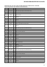
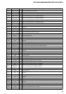
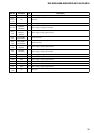
L1 to L5,
L8
SDR_DATA23 to
SDR_DATA20,
SDR_DATA24,
SDR_DATA19
I/O
Serial data input/output with the 256Mbit SD-RAM
L9
NAND_DA4
I/O
Serial date input/output with the NAND flash memory
L10
GND
-
Ground terminal
L11
NC
-
Not used
L17, L18
GND
-
Ground terminal
L19, L22
to L25
LCD_B1 to
LCD_B5
OVideo signal (B) output to the level shift
L26
NC
-
Not used
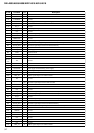
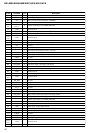
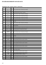
M1 to M5,
M8
SDR_DATA18 to
SDR_DATA13
I/O
Serial data input/output with the 256Mbit SD-RAM
M9
NAND_CEZ0 O Chip enable signal output to the NAND flash memory
M10,
M17, M18
GND
-
Ground terminal
M19 LCD_B0
OVideo signal (B) output to the level shift
M22 to
M25
LCD_G0 to
LCD_G3
O
Video signal (G) output to the level shift
M26
NC
-
Not used
N1 to
N5, N8
SDR_DATA12 to
SDR_DATA7
I/O
Serial data input/output with the 256Mbit SD-RAM
N9, N10,
N17 to
N19
GND
-
Ground terminal
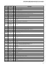
N22, N23
LCD_G4, LCD_G5
O
Video signal (G) output to the level shift
N24, N25
LCD_R0, LCD_R1
OVideo signal (R) output to the level shift
N26
VMICIN
I
Power supply voltage input terminal
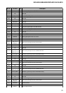
P1 to P4
SDR_DATA5 to
SDR_DATA2
I/O
Serial data input/output with the 256Mbit SD-RAM
P5
SDR_DQM0
O
Write mask signal output to the 256Mbit SD-RAM
P8
SDR_DATA6
I/O
Serial data input/output with the 256Mbit SD-RAM
P9
GND
-
Ground terminal
P10
RESETZ O Reset signal output to the USB controller
P17 to P19 GND
-
Ground terminal
P22 LCD_R3 O
Video signal (R) output to the level shift