


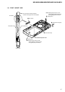

NW-A805/A806/A808/NWZ-A815/A816/A818
1919
NW-A805/A806/A808/NWZ-A815/A816/A818
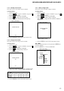
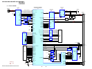
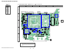
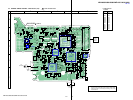
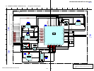
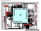
• Note for Printed Wiring Boards and Schematic Diagrams
• MAIN board is multi-layer printed board.
However, the patterns of intermediate-layers have not been
included in diagrams.
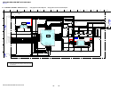
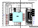
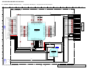
Note on Schematic Diagram:
• All capacitors are in µF unless otherwise noted. (p: pF)
50 WV or less are not indicated except for electrolytics
and tantalums.
• All resistors are in Ω and
1
/
4
W or less unless otherwise
specified.
• C : panel designation.
• A : B+ Line.
• Power voltage is dc 3.7 V and fed with regulated dc power
supply from CN901 pin 1 and pin 2 on the MAIN board.
• Voltages are dc with respect to ground under no-signal
conditions.
no mark : PLAY BACK
• Voltages are taken with a VOM (Input impedance 10 MΩ).
Voltage variations may be noted due to normal produc-
tion tolerances.
• Signal path.
F : AUDIO
L : VIDEO
• Abbreviation
FR : French model
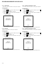
Note on Printed Wiring Board:
• Y : parts extracted from the conductor side.
• : Pattern from the side which enables seeing.
(The other layers' patterns are not indicated.)
Caution:
Pattern face side: Parts on the pattern face side seen from
(Side B) the pattern face are indicated.
Parts face side: Parts on the parts face side seen from
(Side A) the parts face are indicated.
Ver. 1.2