


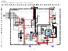
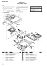

54
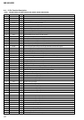
MZ-N510CK
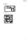
Pin No.
111
112
113
114, 115
116
117
118
119, 120
121
122
123
124
125
126
127
128
129
130
131
132
133
134
135
136
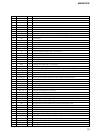
137
138
139, 140
141
142
143
144
145
146
147
148
149
150
151
152
153
154, 155
156
157
158
159
160
161
162, 163
164
165
I/O
O
O
O
O
O
O
O
O
I
O
O
O
O
O
O
O
I
O
I
I
I
O
O
I
I
O
O
O
O
O
O
O
O
O
O
O
O
I
I
I
O
I/O
O
I
I
I
I
I
I
I
Pin Name
BATT_CTL
VREC_CTL
XRST_CHG_IC
PD_S0, 1
LINK_MON
PL_CTL
GND_SW
NC
SLD_MON
NC
SLEEP
FFCLR
CHGI_CTL1
CHGI_CTL2
ORANGE_LED
CHG_LED
XTEST
XRF_RST
XEXT_PWR
XHOLD_SW
COUT_MON
CHG_ADSEL
CHGI_SEL
XDC_IN
SPDL_MON
XCS_PWR_IC
D_EN1, 2
XCS_LCD
LCD_STB
XRST_MTR_DRV
XCS_NV
CHG_PWM
VREC_PWM
NC
NJM_XMUTE
D_VO_PWM
XCS_REC_DRV
T_MARK _SW
JOG_A
JOG_B
NC
SSB_DATA
SSB_CLK
VBUS_DET
VB_MON
CHG_MON
VREF_MON
SET_KEY_1, 2
CRADLE_DET
HIDC_MON
Description
Control signal output for the voltage step up circuit in the external battery case Not used (open)
VREC voltage control signal output Not used (open)
Reset signal output to the battery charge control IC
PD IC mode changeover signal output to the optical pick up
Linking area monitor signal output Not used (open)
Plunger control signal output Not used (open)
Ground changeover switch control signal output Not used (open)
Not used (open)
Sled servo monitor signal input
Not used (open)
System sleep control signal output to the power control
Input latch output for the start switching to the power control
Charge current limit ON/OFF control signal output at the time of adaptor use
Charge current limit value changeover control signal output at the time of adaptor use Not used (open)
Orange LED ON/OFF control signal output Not used (open)
LED ON/OFF control signal output for CHG (charge display) Not used (open)
Terminal for the test mode setting (normally open) “L”: test mode
Reset control signal output to the RF amplifier “L”: reset
External power supply (AC adaptor/charging stand) detection signal input
HOLD switch input terminal “L”: hold ON
Traverse count measurement monitor input
A/D terminal of the battery charge contro IC output selection signal output
Charge/discharge changeover control signal output for the current sense amplifier
DC plug detection signal input Not used (open)
Spindle servo monitor signal input
Chip select signal output to the power control
Control signal output for the D class headphone amplifier Not used (open)
Chip select signal output to the liquid crystal display module
Strobe signal output to the liquid crystal display module
Reset control signal output to the motor driver “L”: reset
Chip select signal output to the nonvolatile memory
Output voltage control signal output to the battery charge control
PWM signal output for the Over write head drive power supply voltage control to the REC driver
PWM signal output for the laser power supply voltage control to the power control Not used (open)
Muting control signal to the headphone amplifier (NJM type made by JRC) Not used (open)
Power supply control signal output for the D class headphone amplifier Not used (open)
Chip select signal output to the REC driver Not used (open)
T MARK (track mark) switch input terminal “L”: track mark detection Not used (open)
Jog dial pulse input from the switch & liquid crystal display module Not used (open)
Jog dial pulse input from the switch & liquid crystal display module Not used (open)
Not used (open)
SSB data input/output with the RF amplifier
SSB clock output to the RF amplifier
USB power supply voltage detection terminal
Voltage monitor input terminal (A/D input) of the UNREG power supply
Decrement of voltage detection and charge/discharge current monitor input from the battery charge control
Reference voltage monitor input (A/D input) from the RF amplifier
Key input (A/D input) from the switch & liquid crystal display module
USB cradle or battery case detection signal input Not used (connected to the ground)
HIGH DC voltage monitor input (A/D input)