


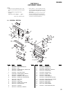

34
NW-MS6
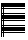
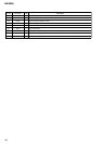
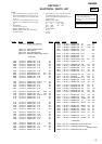
Pin No. Pin Name I/O Description
171 VDDIO2 —
Power supply terminal (+2.8V)
172 VSSIO2 —
Ground terminal
173 to 18
0
FRIO8 to FRIO15
I/O
Not used (open)
181 VDDIO2 —
Power supply terminal (+2.8V)
182 VSSIO2 —
Ground terminal
183 to 187
FRCE0 to FRCE4
O
Not used (pull up)
188 FRWE O
Not used (pull up)
189 FRRE O
Not used (pull up)
190 FRCLE O
Not used (open)
191 FRALE O
Not used (open)
192 FRWP O
Not used (pull up)
193 VDDIO2 —
Power supply terminal (+2.8V)
194 FRREADY I
Not used (fixed at “L”)
195 VSSIO2 —
Ground terminal
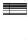
196 VSSIO3 —
Ground terminal
197 FS256 O
Clock signal (11.2896 MHz) output to the D/A converter (IC3100)
198 PCMO O
Digital audio signal output to the D/A converter (IC3100)
199 XCSADA —
Not used (open)
200 CDTO O
Not used (open)
201 CCLK —
Not used (open)
202 DGSDO O
Not used (open)
203 VDDIO3 —
Power supply terminal (+1.8V)
204 BCK O
Bit clock signal output to the D/A converter (IC3100)
205 LRCK O
L/R sampling clock signal output to the D/A converter (IC3100)
206 VSSIO3 —
Ground terminal
207 DGSDI I
Not used (fixed at “L”)
208 CDTI I
Not used (fixed at “L”)
209 PCMI I
Not used (fixed at “L”)
210 VDDIO3 —
Power supply terminal (+1.8V)
211 BUSPLU I
Not used (fixed at “L”)
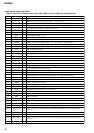
212 to 217 TEST0 to TEST5 I
For test terminal Normally open
218 VSSCORE —
Ground terminal
219, 220 MD6, MD5 I
Mode setting input terminal Fixed at “H” in this set
221 MD4 I
Mode setting input terminal Fixed at “L” in this set
222 MD3 I
Mode setting input terminal Fixed at “H” in this set
223, 224 MD2, MD1 I
Mode setting input terminal Fixed at “L” in this set
225 MD0 I
Mode setting input terminal Fixed at “H” in this set
226 NMI I
Not used (fixed at “L”)
227 VDDCORE —
Power supply terminal (+1.8V)
228 TCLK I
Not used (open)
229 TDI I
Not used (open)
230 TMS I
Not used (open)
231 XTRST I
Not used (open)
232 TCLKD I
Not used (open)
233 TDID I
Not used (open)
234 TMSD I
Not used (open)