


17
NW-MS6
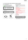
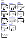
Note on Printed Wiring Boards:
• X : parts extracted from the component side.
• Y : parts extracted from the conductor side.
• : Pattern from the side which enables seeing.
(The other layers' patterns are not indicated.)
Caution:
Pattern face side: Parts on the pattern face side seen from
(Conductor Side) the pattern face are indicated.
Parts face side: Parts on the parts face side seen from
(Component Side) the parts face are indicated.
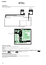
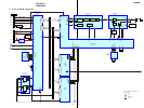
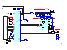
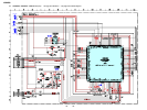
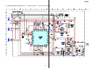
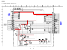
5-3. NOTE FOR PRINTED WIRING BOARDS AND SCHEMATIC DIAGRAMS
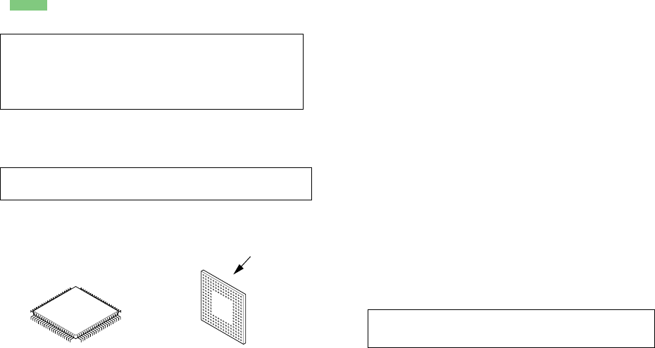
• Lead Layouts
surfac
e
Lead layout of conventional IC CSP (chip size package)
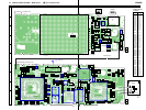
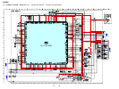
• MAIN board and SUB board are six-layer printed boards.
However, the patterns of layers 2 to 5 have not been included
in these diagrams.
* Replacement of C5000, IC5600, IC7001and IC8000 used
in this set requires a special tool.
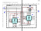
• The voltage and waveform of CSP (chip size package)
cannot be measured, because its lead layout is different
form that of conventional IC.
Note on Schematic Diagram:
• All capacitors are in µF unless otherwise noted. pF: µµF
50 WV or less are not indicated except for electrolytics
and tantalums.
• All resistors are in Ω and
1
/
4
W or less unless otherwise
specified.
• % : indicates tolerance.
• A : B+ Line.
• Power voltage is dc 1.2 V and fed with regulated dc power
supply from battery terminal.
• Voltages and waveforms are dc with respect to ground
under no-signal conditions.
• no mark : PLAYBACK
( ) : when USB connection
• Voltages are taken with a VOM (Input impedance 10 MΩ).
Voltage variations may be noted due to normal produc-
tion tolerances.
• Waveforms are taken with a oscilloscope.
Voltage variations may be noted due to normal produc-
tion tolerances.
• Circled numbers refer to waveforms.
• Signal path.
F : PLAYBACK
E : Check-out
j : Check-in
* Replacement of IC5000, IC5600, IC7001and IC8000
used in this set requires a special tool.