


– 13 –
– 14 –
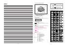
MEMO
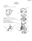
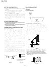
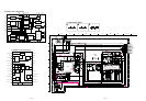
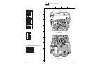
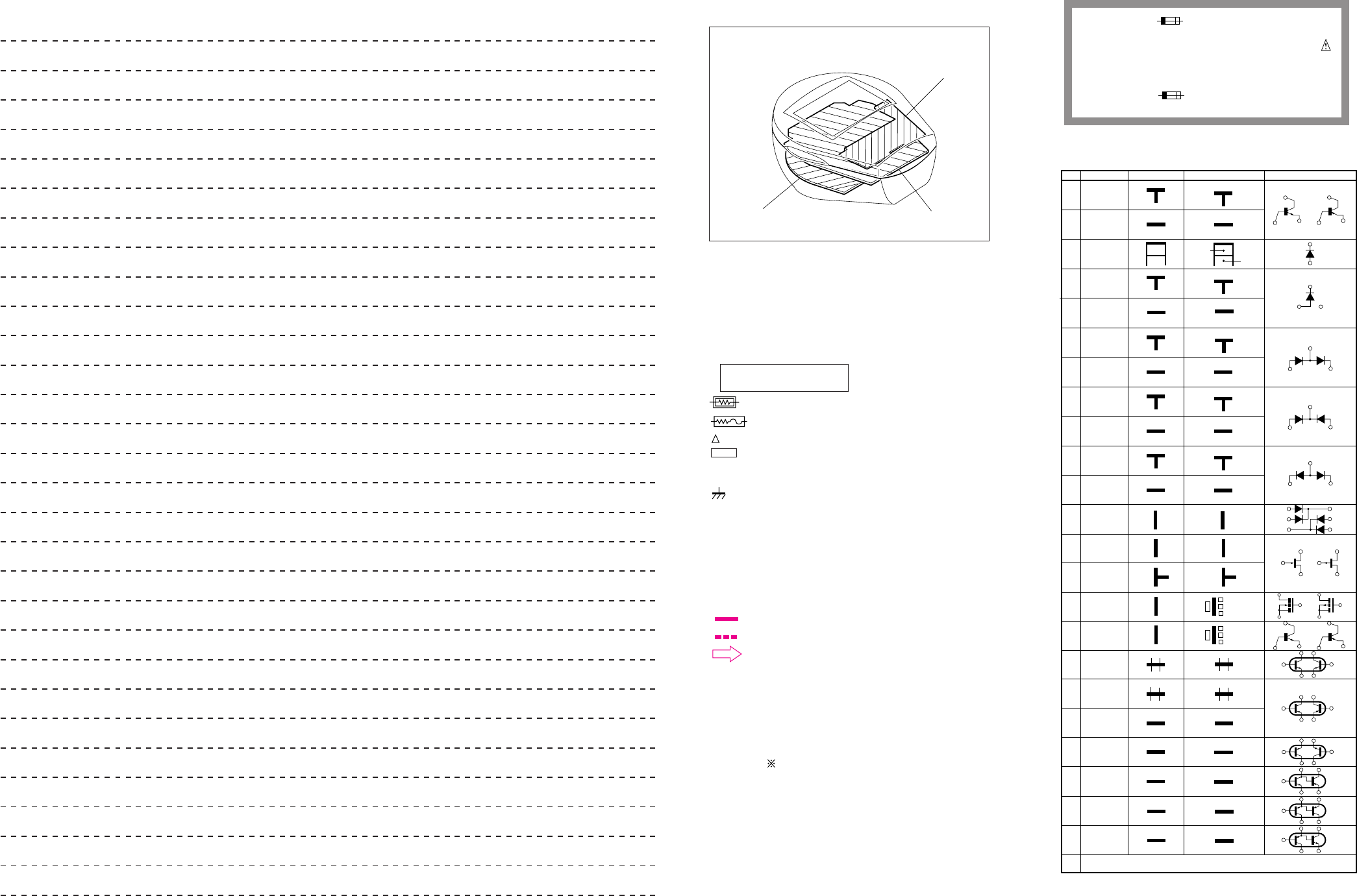
4-3. CIRCUIT BOARDS LOCATION
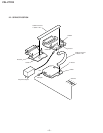
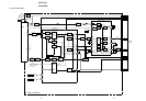
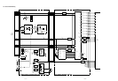
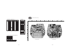
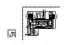
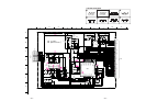
4-4. PRINTED WIRING BOARDS AND
SCHEMATIC DIAGRAMS
Note:
• Capacitors without voltage indication are all 50V.
• All resistors are in ohms.
kΩ=1000Ω, MΩ=1000kΩ
• Indication of resistance, which dose not have one for rating electrical power, is
as follows.
Pitch : 5mm
Rating electrical power :
1
/
4
W
•
: nonflammable resistor.
•
: fusible resistor.
•
: internal component.
•
: panel designation and adjustment for repair.
• All variable and adjustable resistors have characteristic curve B, unless otherwise
noted.
•
: earth-chassis.
• As to the voltage volue shown by the semiconductors on the Shematic Diagram,
see the another list
• Readings are taken with a color-bar signal input.
• Readings are taken with a 10MΩ digital multimeter.
• Voltages are dc with respect to ground unless otherwise noted.
• Voltage variations may be noted due to normal production tolerances.
• All voltages are in V.
• Circled numbers are waveform references.
•
: B+ bus.
•
: B– bus.
• : signal path.
Reference information
RESISTOR : RN METAL FILM
: RC SOLID
: FPRD NONFLAMMABLE CARBON
: FUSE NONFLAMMABLE FUSIBLE
: RW NONFLAMMABLE WIREWOUND
: RS NONFLAMMABLE METAL OXIDE
: RB NONFLAMMABLE CEMENT
:
ADJUSTMENT RESISTOR
COIL : LF-8L MICRO INDUCTOR
CAPACITOR : TA TANTALUM
: PS STYROL
: PP POLYPROPYLENE
: PT MYLAR
: MPS METALIZED POLYESTER
: MPP METALIZED POLYPROPYLENE
: ALB BIPOLAR
: ALT HIGH TEMPERATURE
: ALR HIGH RIPPLE
Note: The symbol display is on the component slde.
The components identified by shading and mark
are critical for safety. Replace only with part number
specified.
The symbol indicate fast operating fuse.
Replace only with fuse of same rating as maked.
G
D
S
B1 E1
C2
B2 C1
E2
2
3
4
5
6
7
8
9
0
!¡
!™
!¢
!§
!¶
!•
–
1
G
D
S
B2 E2
C1
B1 C2
E1
B2 E2
C1
B1 C2
E1
B2 E2
C1
B1 C2
E1
!ª
B1 E1
E2
C1(B2)
C2
@º
B1
E2
C1
C2
@™
@£
(B2)
E1
(B2)
E1
E2
B1
C2
C1
@¡
B1
E1
C2
B2
C1
E2
G
S
S
D
G
D
B1
E1
C2
B2
C1
E2
B1
E2
C2C1(B2)
E2
B1
C1
C2E1(B2)
C2
B1
C1
E2E1(B2)
C2
B1
C1
E2
B2
E1
C2
Ver.1.5
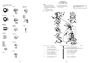
Transistor
(FET)
Transistor
Transistor
Transistor
Transistor
Transistor
Transistor
Transistor
Transistor
Transistor
Discrete semiconductot
(Chip semiconductors that are not actually used are included.)
Diode
Diode
Diode
Diode
Diode
Diode
Diode
Diode
Diode
Diode
Source
Source
Anode
Anode
(NC)
(NC)
Cathode
Anode
Cathode
Common
Cathode
Cathode
Common
Cathode
Cathode
Common
Common
Common
Common
Cathode
Anode
Base
Emitter
Collector
Base
Emitter
Collector
Drain
Gate
Gate
Drain
Device Printed symbol Terminal name
Circuit
Terminal name of semiconductors in silk screen
printed circuit (
*
)
Anode
Anode
Anode Cathode
Anode Anode
Cathode
!£
Transistor
(FET)
Transistor
(FET)
!∞
Emitter
Collector
Base
Transistor
Source
Gate
Drain
Cathode
Anode
Anode
Cathode
Anode
Anode
A
B
T1