


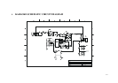
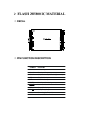
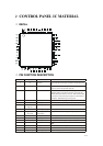
CONTROL PANEL IC MATERIAL
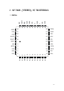
DECAL
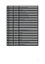
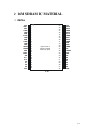
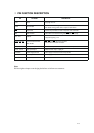
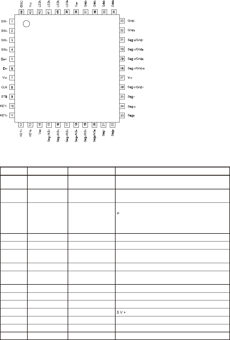
PIN FUNCTION DESCRIPTION
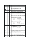
Pin No. Symbol Pin Name Description
6D
IN
Data input Inputs serial data at rising edge of shift clock, starting from lower
bit.
5D
OUT
Data output Outputs serial data at falling edge of shift clock, starting from
lower bit. This is N-ch open-drain output pin.
9 STB Strobe Initializes serial interface at rising or falling edge to make
Pd16312 waiting for reception of command. Data input after
STB has fallen is processed as command. While command data
is processed, current processing is stopped, and serial interface
is initialized. While STB is high, CLK is ignored.
8 CLK Clock input Reads serial data at rising edge, and outputs data at falling edge.
44 OSC Oscillator pin Connect resistor for determining oscillation frequency to this pin.
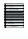
15 to 20 Seg
1
/KS
1
to
Seg
6
/KS
6
High-voltage output Segment output pins (Dual function as key source)
37 To 32 Grid
1
to Grid
6
High-voltage output (grid) Grid output pins
26,28 to 31 Seg
12
/Grid
11
to
Seg
16
/Grid
7
High-voltage output
(segment/grid)
These pins are selectable for segment or grid output.
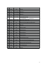
42 to 39 LED
1
to LED
5
LED output CMOS output. +20 mA max.
10 to 13 Key
1
to Key
4
Key data input Data input to these pins is latched at end of display cycle.
1 to 4 SW
1
to SW
4
Switch input These pins constitute 4-bit general-purpose input port.
14, 38 V
DD
Logic power
±
10 %
7, 43
V
SS
Logic ground Connect this pin to GND of system.
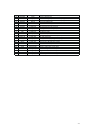
27 V
EE
Pull-down level
V
DD
−
35 V max.
21 to 25
Seg7 to Seg11
High-voltage output
Segment output pins.
4-13