20
SA-FT7ED/WFT7/SS-CNF7ED/FRF7ED/WS-FT7
1 VSENSE I Terminal for detection of AC line voltage.
2 F/B I Terminal for frequency modulation with FB.
3CTICapacitor for oscillator.
4RTIOscillator frequency setting resistor
5 GND — Ground
6 TIMER I Capacitor determines the period of abnormal detection.
7SSICapacitor for a soft start timing.
8 VC1 I Power supply terminal for the control circuit.
9 OCP I Terminal for over current detection and didt protection.
10 VC2 O Power supply terminal for a driver.
11 P_GND — Ground for low side driver.
12 VG_L O Output of low side driver.
13 — — Not used. (Open)
14 VB O Power supply terminal for high side driver.
15 VS I Reference voltage terminal for high side driver.
16 VG_H O Output of high side driver.
17 — — Not used. (Open)
18 VD I Terminal for Drain-Kick starting.
• IC Pin Description
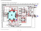
IC101 CXD9841P (DC-DC CONVERTER) (POWER Board)
Pin No. Pin Name I/O Pin Description


