


10
SA-FT7ED/WFT7/SS-CNF7ED/FRF7ED/WS-FT7
SECTION 3
DIAGRAMS
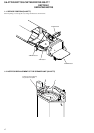
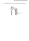
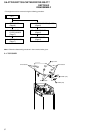
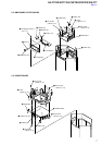
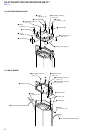
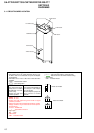
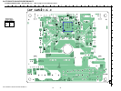
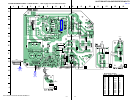
3-1. CIRCUIT BOARDS LOCATION
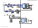
Note on Schematic Diagram:
• All capacitors are in µF unless otherwise noted. (p: pF)
50 WV or less are not indicated except for electrolytics
and tantalums.
• All resistors are in Ω and
1
/
4
W or less unless otherwise
specified.
• 2 : nonflammable resistor.
• C : panel designation.
Note:
The components identi-
fied by mark 0 or dotted
line with mark 0 are criti-
cal for safety.
Replace only with part
number specified.
Note:
Les composants identifiés par
une marque 0 sont critiques
pour la sécurité.
Ne les remplacer que par une
piéce portant le numéro
spécifié.
• A : B+ Line.
• B : B– Line.
•Voltage is dc with respect to ground under no-signal
(detuned) condition.
•Voltages are taken with a VOM (Input impedance 10 MΩ).
Voltage variations may be noted due to normal produc-
tion tolerances.
no mark : POWER ON
∗
: Impossible to measure
• Signal path.
F : LINE
• Abbreviation
CND : Canadian model.
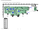
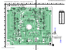
Note on Printed Wiring Boards:
• X : parts extracted from the component side.
• : Pattern from the side which enables seeing.
• Abbreviation
CND : Canadian model.
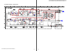
C
B
These are omitted.
E
Q
B
These are omitted.
C
Q
Q
E
BCE
LED boar
d
SW board
AMP board
FILTER board
POWER board
ACIN board
INPUT board