


– 10 –
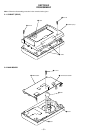
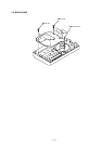
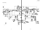
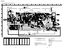
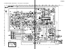
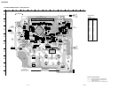
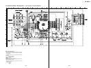
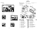
SECTION 4
DIAGRAMS
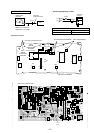
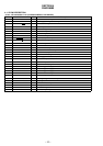
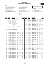
4-1. IC PIN DESCRIPTION
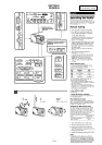
• IC201 uPD17072GB-017-1A7 (SYSTEM CONTROL, LCD DRIVER)
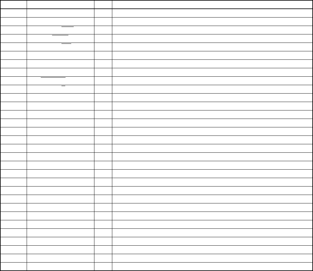
Pin No. Pin Name I/O Pin Description
1 CS O EEPROM CS control output
2 POWER O Power supply (for signal ) start output H: Radio ON L: Radio OFF
3 BAR/ROD O Antenna switch output H: BAR ANTENNA L: ROD ANTENNA
4 MUTE O MUTE output H: MUTE OFF L: MUTE ON
5 AM/FM O Band switch signal output H: SW, MW, LW L: FM
6 – 9 KS0 – 3 O Key source output
10 – 13 KR0 – 3 I Key return input
14 INITIAL O 9K/10K read output
15 NORMAL/FINE I Frequency step switch input H: FINE L: NORMAL
16 H/L O SW filter switch signal output H: SW L: FM, MW. LW
17 10.25 O Attenator output
18 GND — GND
19 EO O Tuner PLL error output
20 VCOL (LW/MW/SW) I VCO (SW/MW/LW band) input
21 VCOH (FM) I VCO (FM band) input
22 REG0 — Capacitor terminal (regulator circuit)
23 VDD — Power supply terminal (+2.7 V)
24 XOUT O Oscillation output (75 kHz)
25 XIN I Oscillation input (75 kHz)
26 REG1 — Capacitor terminal (regulator circuit)
27 REGLCD0 — LCD driving power supply terminal
28, 29 CAPLCD0, 1 — LCD driving power supply terminal
30 REGLCD1 — LCD driving power supply terminal
31 – 34 COM0 – 3 O LCD drive common output
35 – 49 LCD0 – 14 O LCD drive segment output
50, 51 VDET1, 2 I Reducing voltage information input
52 BEEP O Beep output
53 TUNE I Receive information input
54 HOLD I Hold input
55 SCK O Serial clock output
56 DI/DO I/O Serial data input/output