


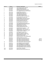
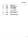
Troubleshooting
Samsung Electronics 2-7
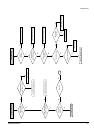
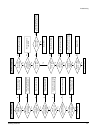
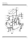
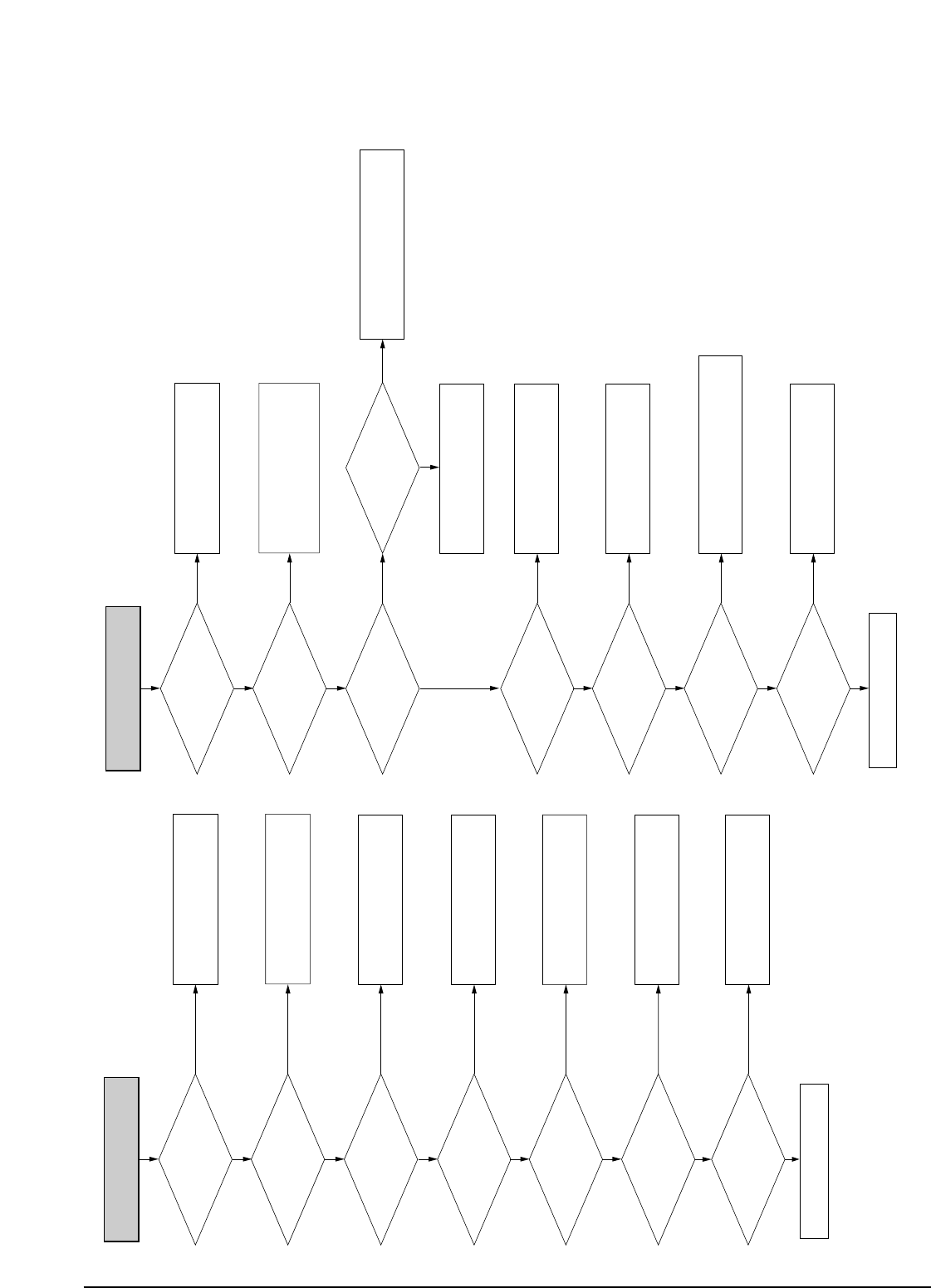
Battery charging error
VDD and 5V
appears at pin5 in
PIC03?
pin2,4 in PQ502
is in low state?
Base in PQ503
is in high state?
Check the connection to
pin8 in PIC04.
Check the connection between
pin base in PQ503 and pin48 in UIC01.
Yes
No
No No
Collector in PQ505
is in low state?
Yes
Yes
No
Pin33 in
UIC01 is in
high state?
Yes
No
VDD appears at
pin10,24,35 in
UIC01?
Yes
Change PQ505 and PR506.
Change PQ503
Check the connection betwen
pin33 in UIC01 and pin2 in PJ501.
Check the connection between
pin10,24,35 in UIC01 and pin1 in PIC04.
No
Pin30 in UIC01
is in high state?
Check the connection between
pin4 in PIC03 and pin30 in UIC01.
Yes
No
Yes
8.38MHz is normal
at pin40,41, in UIC01?
No
Yes
Change UXT02.
Check the battery.
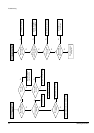
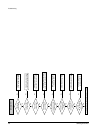
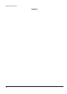
CVBS output error
27MHz clock
input is normal at
pin 161 in ZIC1?
Analog output
is normal at pin 169
in ZIC1?
Check the connection between
pin 161 in ZIC1 and ZX101.
Check the soldering of ZIC1.
Yes
No
No
Analog signals are
inputted normally at
pin4 in VIC01?
Yes
No
Power is
normal at pin 1, 16 in
VIC01.
Yes
No
Yes
Check the connection between
pin 169 in ZIC1 and VIC01.
Check the connection betwen
VIC01 and pin 4 in PQ118.
Pin of DAC VDD25
in ZIC1 has
normal level?
Check the connection to
positive pin in PE120.
Yes
No
Yes
Check the soldering of VIC01.
No
Check the connection between
VIC01 and output jack.
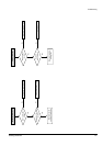
Peak to peak
voltage level of VR104?
Video signal of
about 1V appears at output
jack at pin3?
No
Yes
Check the cable.