


14
SECTION 4
TECHNICAL DESCRIPTION
4.1 GENERAL
The Ray48 can be considered as consisting of two major sections. They are:
• The Control Circuitry (considering of the front panel controls, the LCD display,
control CPU)
• The Transmitter/Receiver/PLL circuits
4.2 THE CONTROL SECTION
The heart of the control section is the CPU IC201, located on the Front PCB.
The CPU controls all of the following items:
•
Controls the Squelch circuit by detecting a busy signal from the second IF circuit IC5.
• Generates a beep tone when a key is activated on the keyboard.
• Mutes the transmitter modulation circuit when receiving.
• Controls the output power of the transmitter High/Low.
• Controls the dividing ratio N of the PLL circuit.
• Switches On/Off the transmitter power.
• Mutes AF audio.
• Detects a weather alert signal (when in Monitor Mode).
• Controls the LCD display.
4.3 THE TRANSMITTER/RECEIVER/PLL SECTIONS
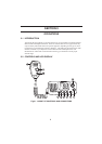
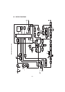
In reading through the following circuit descriptions, it may be helpful to refer to Figure 4-1
Block Diagram of the TX/RX/PLL circuits.
4.3.1 PLL (Phase Lock Loop Circuit)
The PLL circuit is the frequency synthesizer in the Ray48.
The reference frequency of 12.8 MHz is provided by crystal XTL1 and IC3. IC3 contains
the reference oscillator (12.8 MHz) circuit, the phase comparator, the program counter and
the phase detector. The 12.8 MHz reference signal is divided by 512 in the program counter
in IC3 to obtain a 25 KHz reference signal. The dividing ratio is determined by CPU IC201.
The VCO output from oscillator Q4 is amplified by buffer amplifier Q3, and returned to IC3
and is divided by the dividing ratio N to obtain a 25 KHz signal. N for 1N in IC3 is
determined by CPU IC201. Both of these 25 KHz signals are fed into the phase comparator
circuit of IC3.
The phase detected signal, obtained by comparing the two 25 KHz signals the same phase.
When this condition is met, the PLL circuit is locked. If the two signals have a large phase
difference, the PLL is unlocked. In this condition, the unlocked signal is fed to CPU IC201
from IC3 and the transmitter is compelled to stop.
The VCO output from Q4 is fed to the TX amplifier Q2 and the first RX mixer Q19 through
buffer amplifier Q3.