


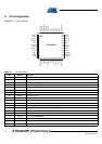

4
4994BS–AUDR–05/08
ATR4262M1 [Preliminary]
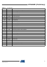
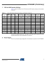
3. Absolute Maximum Ratings
Stresses beyond those listed under “Absolute Maximum Ratings” may cause permanent damage to the device. This is a stress rating
only and functional operation of the device at these or any other conditions beyond those indicated in the operational sections of this
specification is not implied. Exposure to absolute maximum rating conditions for extended periods may affect device reliability.
Parameters Pin Group Min. Max. Unit
Voltage
Digital –0.5 +5.5 V
Supply –0.5 +12 V
Voltage references –0.5 +6.4 V
SW1, SW3 –0.5 +12 V
SW2 –0.5 V
S
+ 0.5 V
SW4, SW5, SW6, SW7 –0.5 + 5.5 V
Mixer outputs –0.5 +16 V
Analog –0.5 V
S
+ 0.5 V
Current Switches 0 2.7 mA
Ambient temperature T
amb
–40 +100 °C
Storage temperature T
stg
–40 +100 °C
Junction temperature T
j
+150 °C
Power dissipation P
tot
1.4 W
ESD HBM All pins –2 +2 kV
ESD MM All pins –200 +200 V
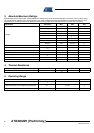
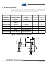
4. Thermal Resistance
Parameters Test Condition Symbol Value Unit
Thermal resistance junction-ambient Soldered to PCB R
thJA
30 K/W
5. Operating Range
Parameters Symbol Value Unit
Supply voltage V
S
8 to 10 V
Supply voltage for operation of control bus
(data preservation in bus registers is guaranteed)
V
S
7 to 10 V
Ambient temperature T
amb
–40 to +90 °C